Click to expand full text
HD74AC165/HD74ACT165
Parallel-Load 8-bit Shift Register
Description
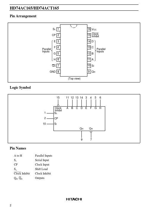
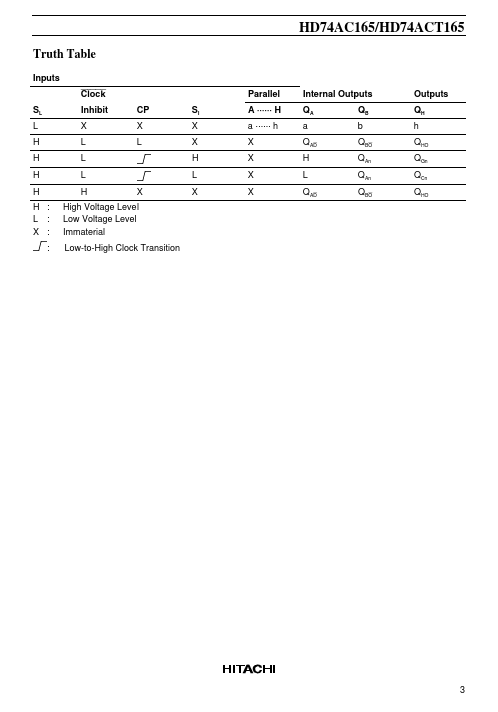
This 8-bit serial shift register shifts data from Q A to QH when clocked, Parallel inputs to each stage are enabled by a low level at the Shift/Load Input. Also included is a gated clock input and a complementary output from the eighth bit. Clocking is accomplished through a 2-input NOR gate permitting one input to be used as a clock inhibit function. Holding either of the clock inputs high inhibits clocking, and holding either clock input low with the Shift/Load input high enables the other clock input. Data transfer occurs on the positive going edge of the clock. Parallel loading is inhibited as long as the Shift/Load input is high.
 HD74AC165 Datasheet