Datasheet Details
| Part number | FDZ371PZ |
|---|---|
| Manufacturer | Fairchild (now onsemi) |
| File Size | 311.71 KB |
| Description | Thin WL-CSP MOSFET |
| Datasheet |
 FDZ371PZ Datasheet FDZ371PZ Datasheet
|
|
|
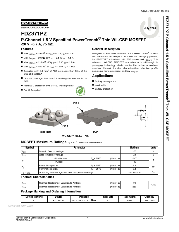
Designed on Fairchild's advanced 1.5 V PowerTrench® process with state of the art "fine pitch" Thin WLCSP packaging process, the FDZ371PZ minimizes both PCB space and rDS(on).
| Part number | FDZ371PZ |
|---|---|
| Manufacturer | Fairchild (now onsemi) |
| File Size | 311.71 KB |
| Description | Thin WL-CSP MOSFET |
| Datasheet |
FDZ371PZ Datasheet
|
|
|
|
Note: Below is a high-fidelity text extraction (approx. 800 characters) for FDZ371PZ. For precise diagrams, and layout, please refer to the original PDF.
FDZ371PZ P-Channel 1.5 V Specified PowerTrench® Thin WL-CSP MOSFET July 2009 FDZ371PZ P-Channel 1.5 V Specified PowerTrench Thin WL-CSP MOSFET -20 V, -3.7 A, 75 mΩ Featur...
| Part Number | Description |
|---|---|
| FDZ372NZ | N-Channel 1.5 V Specified PowerTrench Thin WL-CSP MOSFET |
| FDZ375P | P-Channel 1.5V Specified PowerTrench Thin WL-CSP MOSFET |
| FDZ391P | Thin WL-CSP MOSFET |
| FDZ3N513ZT | 30V Integrated NMOS And Schottky Diode |
| FDZ1040L | Integrated Load Switch |
| FDZ1323NZ | MOSFET |
| FDZ1416NZ | MOSFET |
| FDZ1905PZ | P-Channel MOSFET |
| FDZ191P | P-Channel 1.5V PowerTrench WL-CSP MOSFET |
| FDZ192NZ | N-Channel 1.5 V Specified PowerTrench Thin WL-CSP MOSFET |