FDMC15N06 Datasheet Text
FDMC15N06 N-Channel MOSFET
July 2009
FDMC15N06
N-Channel MOSFET
55V, 15A, 0.090Ω Features
- RDS(on) = 0.075Ω ( Typ.)@ VGS = 10V, ID = 15A
- 100% Avalanche Tested
- RoHS pliant
Description
These N-Channel power MOSFETs are manufactured using the innovative UItraFET process. This advanced process technology achieves the lowest possible on-resistance per silicon area, resulting in outstanding performance.This device is capable of withstanding high energy in the avalanche mode and the diode exhibits very low reverse recovery time and stored charge. It was designed for use in applications where power efficiency is important, such as switching regulators, switching converters, motor drivers, relay drivers, lowvoltage bus switches, and power management in portable and battery-operated products.
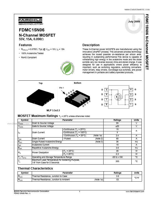
Top Pin 1 S S S G
Bottom D D D D D 5 6 7 8 4 3 2 1 G S S S
D
D
D
MLP 3.3x3.3
MOSFET Maximum Ratings TC = 25oC unless otherwise noted
Symbol VDSS .. VGSS ID IDM EAS IAR EAR PD TJ, TSTG TL Parameter Drain to Source Voltage Gate to Source Voltage -Continuous (TC = 25oC) Drain Current Drain Current Single Pulsed Avalanche Energy Avalanche Current Repetitive Avalanche Energy Power Dissipation (TA = 25oC) (TC = 25oC) -Continuous (TC = 100oC)
- Continuous (TA = 25oC)
- Pulsed (Note 1a) (Note 2) (Note 3) Ratings 55 ±20 15 9 2.4 60 36 15 3.5 35 2.3 -55 to +150 300 Units V V A A A mJ A mJ W W o o
Operating and Storage Temperature Range Maximum Lead Temperature for Soldering Purpose, 1/8” from Case for 5 Seconds
C C
Thermal Characteristics
Symbol RθJC RθJA Parameter Thermal Resistance, Junction to Case Thermal Resistance, Junction to Ambient (Note 1a) Ratings 3.5 53 Units o
C/W
©2009 Fairchild Semiconductor Corporation FDMC15N06 Rev....