Click to expand full text
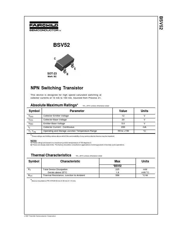
BSV52
BSV52
C
E
SOT-23
Mark: B2
B
NPN Switching Transistor
This device is designed for high speed saturated switching at collector currents of 10 mA to 100 mA. Sourced from Process 21.
Absolute Maximum Ratings*
Symbol
VCEO VCES VEBO IC TJ, Tstg Collector-Emitter Voltage Collector-Base Voltage Emitter-Base Voltage Collector Current - Continuous
TA = 25°C unless otherwise noted
Parameter
Value
12 20 5.0 200 -55 to +150
Units
V V V mA °C
Operating and Storage Junction Temperature Range
*These ratings are limiting values above which the serviceability of any semiconductor device may be impaired.
NOTES: 1) These ratings are based on a maximum junction temperature of 150 degrees C. 2) These are steady state limits.
 BSV52 Datasheet