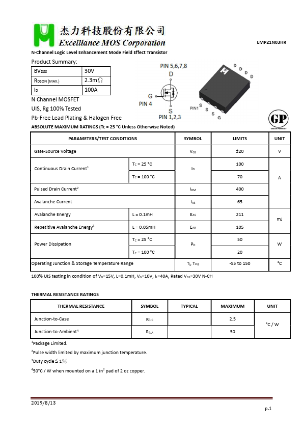
EMP21N03HR
N-Channel Logic Level Enhancement Mode Field Effect Transistor
Product Summary:
BVDSS
30V
RDSON (MAX.)
2.3mΩ
100A
N Channel MOSFET
UIS, Rg 100% Tested
Pb-Free Lead Plating & Halogen Free
ABSOLUTE MAXIMUM RATINGS (Tc = 25 °C Unless Otherwise Noted)
PARAMETERS/TEST CONDITIONS
SYMBOL
Gate-Source Voltage
Continuous Drain Current1 Pulsed Drain Current2
TC = 25 °C ID
TC = 100 °C
Avalanche Current
Avalanche Energy Repetitive Avalanche Energy3
L = 0.1m H
L = 0.05m H
Power Dissipation
TC = 25 °C TC = 100 °C
Operating Junction & Storage Temperature Range
PD Tj, Tstg
100% UIS testing in condition of VD=15V, L=0.1m H, VG=10V, IL=40A, Rated VDS=30V N-CH
LIMITS ±20 100 70 400 65 211 105 50 20
-55 to 150
UNIT V A m J W °C
THERMAL RESISTANCE RATINGS THERMAL RESISTANCE
SYMBOL
Junction-to-Case
RJC
Junction-to-Ambient4...