Click to expand full text
PLL502-02
Low Phase Noise VCXO (24MHz to 50MHz)
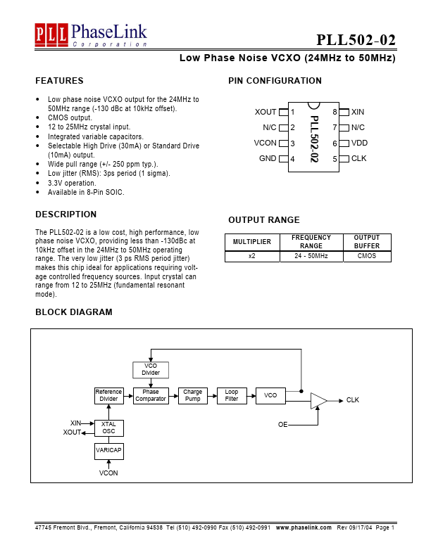
FEATURES
• • • • • • • • • Low phase noise VCXO output for the 24MHz to 50MHz range (-130 dBc at 10kHz offset). CMOS output. 12 to 25MHz crystal input. Integrated variable capacitors. Selectable High Drive (30mA) or Standard Drive (10mA) output. Wide pull range (+/- 250 ppm typ.). Low jitter (RMS): 3ps period (1 sigma). 3.3V operation. Available in 8-Pin SOIC.
PIN CONFIGURATION
XOUT N/C VCON GND
1 2 3 4
8 7 6 5
XIN N/C VDD CLK
PLL502-02
DESCRIPTION
The PLL502-02 is a low cost, high performance, low phase noise VCXO, providing less than -130dBc at 10kHz offset in the 24MHz to 50MHz operating range. The very low jitter (3 ps RMS period jitter) makes this chip ideal for applications requiring voltage controlled frequency sources.
 PLL502-02 Datasheet