Datasheet Details
| Part number | 74AHC125S14 |
|---|---|
| Manufacturer | Diodes Incorporated |
| File Size | 303.81 KB |
| Description | QUADRUPLE 3-STATE BUFFER |
| Datasheet |
 74AHC125S14 Datasheet 74AHC125S14 Datasheet
|
|
|
Download the 74AHC125S14 datasheet PDF. This datasheet also covers the 74AHC125 variant, as both devices belong to the same quadruple 3-state buffer family and are provided as variant models within a single manufacturer datasheet.
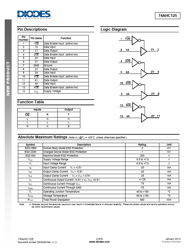
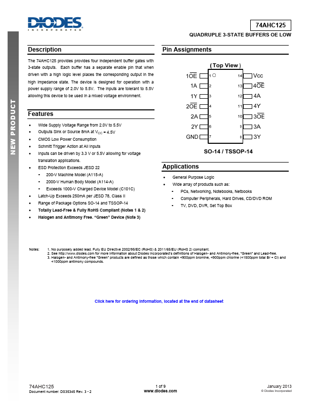
The 74AHC125 provides provides four independent buffer gates with 3-state outputs.
Each buffer has a separate enable pin that when driven with a high logic level places the corresponding output in the high impedance state.
| Part number | 74AHC125S14 |
|---|---|
| Manufacturer | Diodes Incorporated |
| File Size | 303.81 KB |
| Description | QUADRUPLE 3-STATE BUFFER |
| Datasheet |
74AHC125S14 Datasheet
|
|
|
|
Note: Below is a high-fidelity text extraction (approx. 800 characters) for 74AHC125S14. For precise diagrams, and layout, please refer to the original PDF.
NEW PRODUCT 74AHC125 QUADRUPLE 3-STATE BUFFERS OE LOW Description The 74AHC125 provides provides four independent buffer gates with 3-state outputs. Each buffer has a sep...
| Part Number | Description |
|---|---|
| 74AHC125 | QUADRUPLE 3-STATE BUFFER |
| 74AHC125T14 | QUADRUPLE 3-STATE BUFFER |
| 74AHC126 | QUADRUPLE 3-STATE BUFFER |
| 74AHC138 | 3-TO-8 LINE DECODER DEMULTIPLEXER |
| 74AHC138S16 | 3-TO-8 LINE DECODER DEMULTIPLEXER |
| 74AHC138T16 | 3-TO-8 LINE DECODER DEMULTIPLEXER |
| 74AHC14 | HEX INVERTERS |
| 74AHC14S14 | HEX INVERTERS |
| 74AHC14T14 | HEX INVERTERS |
| 74AHC1G00 | SINGLE 2 INPUT POSITIVE NAND GATE |