Datasheet Details
| Part number | Z9973 |
|---|---|
| Manufacturer | Cypress (Infineon) |
| File Size | 129.10 KB |
| Description | Multi-Output Zero Delay Buffer |
| Datasheet |
 Z9973 Datasheet Z9973 Datasheet
|
|
|
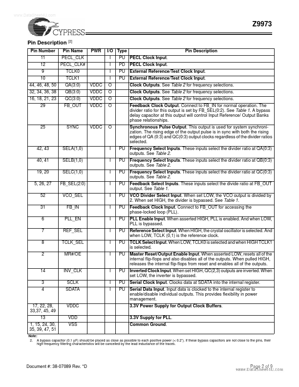
Pin Number 11 12 9 10 44, 46, 48, 50 32, 34, 36, 38 16, 18, 21, 23 29 Pin Name PECL_CLK PECL_CLK# TCLK0 TCLK1 QA(3:0) QB(3:0) QC(3:0) FB_OUT VDDC VDDC VDDC VDDC PWR I/O Type I I I I O O O O PU PD PU PU PECL Clock Input.
PECL Clock Input.
External Reference/Test Clock Input.
| Part number | Z9973 |
|---|---|
| Manufacturer | Cypress (Infineon) |
| File Size | 129.10 KB |
| Description | Multi-Output Zero Delay Buffer |
| Datasheet |
Z9973 Datasheet
|
|
|
|
| Part Number | Description | Manufacturer |
|---|
| Part Number | Description |
|---|---|
| Z9972 | 3.3V/ 125-MHz/ Multi-Output Zero Delay Buffer |
| Z9960 | 200 MHz Multi-Output Zero Delay Buffer |
The following content is an automatically extracted verbatim text from the original manufacturer datasheet and is provided for reference purposes only.