Datasheet4U Logo Datasheet4U.com

Z9960 - 200 MHz Multi-Output Zero Delay Buffer

Description

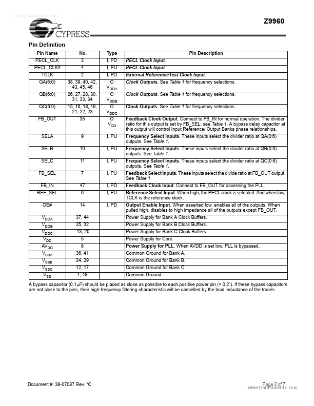
A bypass capacitor (0.1µF) should be placed as close as possible to each positive power pin (< 0.2”).
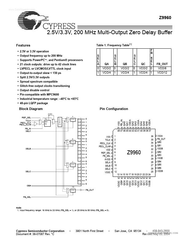
Features

  • 2.5V or 3.3V operation.
  • Output frequency up to 200 MHz.
  • Supports PowerPC, and Pentium® processors.
  • 21 clock outputs: drive up to 42 clock lines.
  • LVPECL or LVCMOS/LVTTL clock input.
  • Output-to-output skew < 150 ps.
  • Split 2.5V/3.3V outputs.
  • Spread spectrum compatible.
  • Glitch-free output clocks transitioning.
  • Output disable control.
  • Pin-compatible with MPC9600.
  • Industrial temperature range:.

📥 Download Datasheet

Full PDF Text Transcription (Reference)

The following content is an automatically extracted verbatim text from the original manufacturer datasheet and is provided for reference purposes only.

View original datasheet text
www.DataSheet4U.com Z9960 2.5V/3.3V, 200 MHz Multi-Output Zero Delay Buffer Features • 2.5V or 3.3V operation • Output frequency up to 200 MHz • Supports PowerPC, and Pentium® processors • 21 clock outputs: drive up to 42 clock lines • LVPECL or LVCMOS/LVTTL clock input • Output-to-output skew < 150 ps • Split 2.5V/3.3V outputs • Spread spectrum compatible • Glitch-free output clocks transitioning • Output disable control • Pin-compatible with MPC9600 • Industrial temperature range: –40°C to +85°C • 48-pin LQFP package S E L A 0 1 S E L B 0 1 S E L C 0 1 Table 1.
Published: |