Datasheet4U Logo Datasheet4U.com

CY7C1525V18 - 1.8V Synchronous Pipelined SRAM

Download the CY7C1525V18 datasheet PDF. This datasheet also covers the CY7C1510V18 variant, as both devices belong to the same 1.8v synchronous pipelined sram family and are provided as variant models within a single manufacturer datasheet.

Features

  • Separate independent read and write data ports.
  • Supports concurrent transactions.
  • 250 MHz clock for high bandwidth.
  • 2-word burst on all accesses.
  • Double Data Rate (DDR) interfaces on both read and write ports (data transferred at 500 MHz) at 250 MHz.
  • Two input clocks (K and K) for precise DDR timing.
  • SRAM uses rising edges only.
  • Two input clocks for output data (C and C) to minimize clock skew and flight time mismatches.
  • Echo clocks (CQ and CQ) simp.

📥 Download Datasheet

Note: The manufacturer provides a single datasheet file (CY7C1510V18-CypressSemiconductor.pdf) that lists specifications for multiple related part numbers.

Full PDF Text Transcription

Click to expand full text
CY7C1510V18, CY7C1525V18 CY7C1512V18, CY7C1514V18 
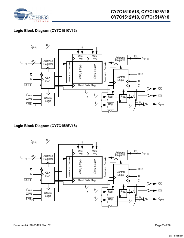
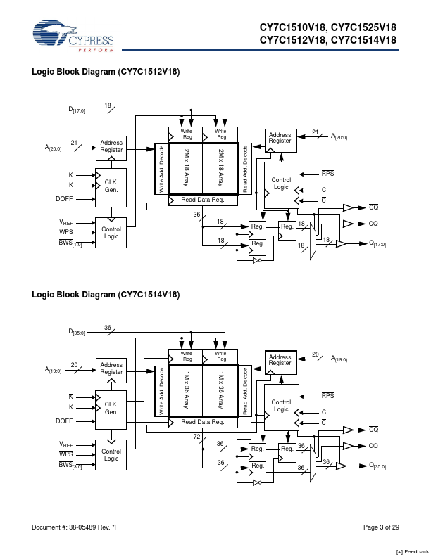
72-Mbit QDR™-II SRAM 2-Word Burst Architecture Features ■ Separate independent read and write data ports ❐ Supports concurrent transactions ■ 250 MHz clock for high bandwidth ■ 2-word burst on all accesses ■ Double Data Rate (DDR) interfaces on both read and write ports (data transferred at 500 MHz) at 250 MHz ■ Two input clocks (K and K) for precise DDR timing ❐ SRAM uses rising edges only ■ Two input clocks for output data (C and C) to minimize clock skew and flight time mismatches ■ Echo clocks (CQ and CQ) simplify data capture in high-speed systems ■ Single multiplexed address input bus latches address inputs for both read and write ports ■ Separate port selects for depth expansion ■ Synchronous internally self-timed writes ■ Availabl
Published: |