(CY7C147xBV25) 72-Mbit (2M x 36/4M x 18/1M x 72) Pipelined SRAM
Full PDF Text Transcription (Reference)
The following content is an automatically extracted verbatim text
from the original manufacturer datasheet and is provided for reference purposes only.
View original datasheet text
CY7C1471BV25
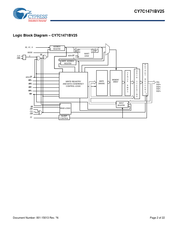
72-Mbit (2 M × 36) Flow-Through SRAM with NoBL™ Architecture
72-Mbit (2 M × 36/1 M × 72) Flow-Through SRAM with NoBL™ Architecture
Features
■ No Bus Latency™ (NoBL™) architecture eliminates dead cycles between write and read cycles
■ Supports up to 133 MHz bus operations with zero wait states ■ Data transfers on every clock ■ Pin compatible and functionally equivalent to ZBT™ devices ■ Internally self timed output buffer control to eliminate the need
to use OE ■ Registered inputs for flow through operation ■ Byte Write capability ■ 2.5-V I/O supply (VDDQ) ■ Fast clock-to-output times
❐ 6.
 CY7C1471BV25 Datasheet