Datasheet Details
| Part number | CY7C1446AV33 |
|---|---|
| Manufacturer | Cypress (Infineon) |
| File Size | 417.46 KB |
| Description | (CY7C144xAV33) Sync SRAM |
| Datasheet |
 CY7C1446AV33 Datasheet CY7C1446AV33 Datasheet
|
|
|
Download the CY7C1446AV33 datasheet PDF. This datasheet also covers the CY7C1440AV33 variant, as both devices belong to the same (cy7c144xav33) sync sram family and are provided as variant models within a single manufacturer datasheet.
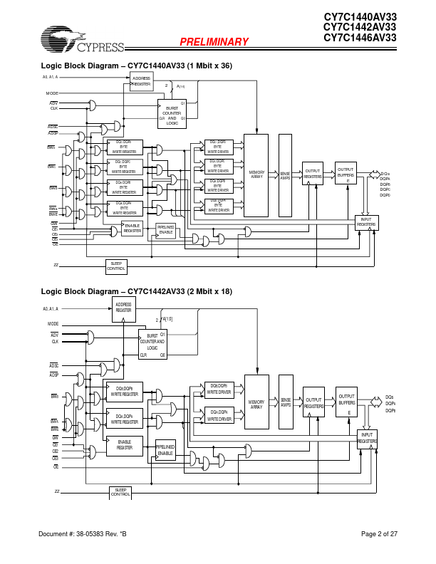
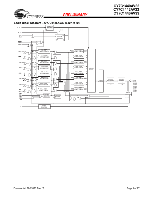
The CY7C1440AV33/CY7C1442AV33/CY7C1446AV33 SRAM integrates 1,048,576 x 36, 2,097,152 x 18 and 524,288 x 72 SRAM cells with advanced synchronous peripheral circuitry and a two-bit counter for internal burst operation.
| Part number | CY7C1446AV33 |
|---|---|
| Manufacturer | Cypress (Infineon) |
| File Size | 417.46 KB |
| Description | (CY7C144xAV33) Sync SRAM |
| Datasheet |
CY7C1446AV33 Datasheet
|
|
|
|
| Part Number | Description | Manufacturer |
|---|---|---|
| CY7C1460SV25 | 36-Mbit (1M x 36/2M x 18) Pipelined SRAM | Cypress |
| CY7C1462SV25 | 36-Mbit (1M x 36/2M x 18) Pipelined SRAM | Cypress |
| CY7C1006D | 1-Mbit (256K x 4) Static RAM | Cypress |
| CY7C1011G | 2-Mbit (128K words x 16 bit) Static RAM | Cypress |
| CY7C1041G | 4-Mbit (256K words x 16 bit) Static RAM | Cypress |
| Part Number | Description |
|---|---|
| CY7C1446AV25 | 36-Mbit Pipelined Sync SRAM |
| CY7C144 | 8K x 9/0 Dual-Port Static RAM |
| CY7C1440AV25 | 36-Mbit Pipelined Sync SRAM |
| CY7C1440AV33 | (CY7C144xAV33) Sync SRAM |
| CY7C1440KV25 | 36-Mbit (1M x 36) Pipelined Sync SRAM |