The following content is an automatically extracted verbatim text
from the original manufacturer datasheet and is provided for reference purposes only.
View original datasheet text
CY7C1441AV33 CY7C1443AV33,CY7C1447AV33
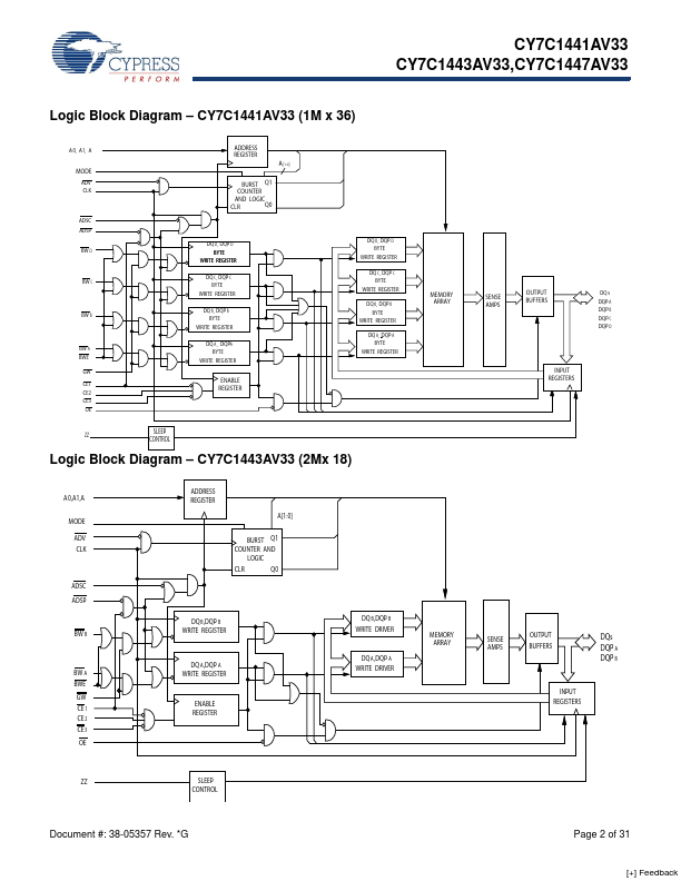
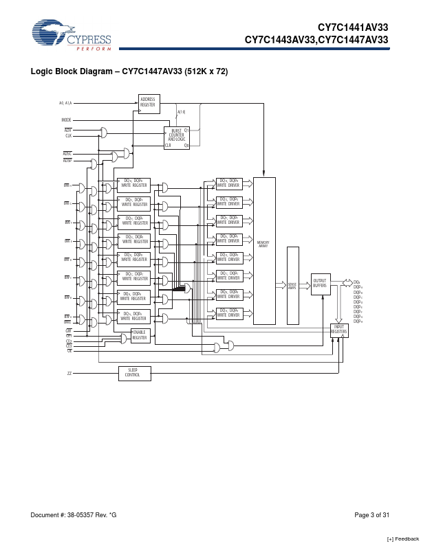
36-Mbit (1M x 36/2M x 18/512K x 72) Flow-Through SRAM
Features
■ Supports 133-MHz bus operations ■ 1M x 36/2M x 18/512K x 72 common IO ■ 3.3V core power supply ■ 2.5V or 3.3V IO power supply ■ Fast clock-to-output times
❐ 6.5 ns (133-MHz version) ■ Provide high-performance 2-1-1-1 access rate ■ User-selectable burst counter supporting Intel® Pentium®
interleaved or linear burst sequences ■ Separate processor and controller address strobes ■ Synchronous self-timed write ■ Asynchronous output enable ■ CY7C1441AV33, CY7C1443AV33 available in
JEDEC-standard Pb-free 100-pin TQFP package, Pb-free and non-lead-free 165-ball FBGA package. CY7C1447AV33 available in Pb-free and non-lead-free 209-ball FBGA package ■ IEEE 1149.
 CY7C1443AV33 Datasheet