Click to expand full text
www.DataSheet4U.com
380CV25
PRELIMINARY
CY7C1380CV25 CY7C1382CV25
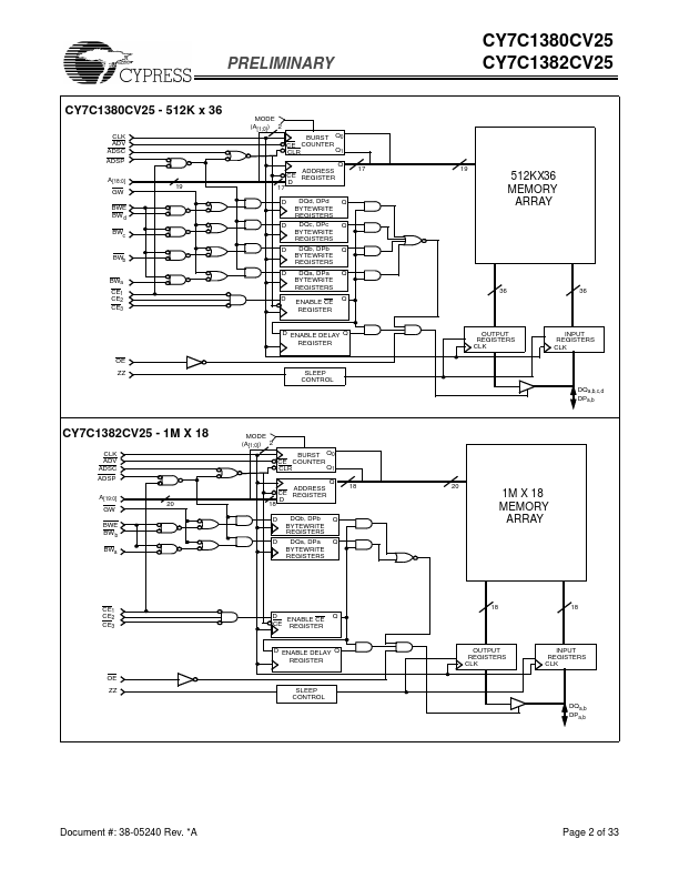
512K x 36/1M x 18 Pipelined SRAM
Features
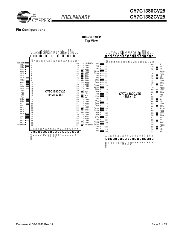
• • • • • • • • • • • Fast clock speed: 250, 225, 200, 167 MHz Provide high-performance 3-1-1-1 access rate Fast OE access times: 2.6, 2.8, 3.0, 3.4 ns Optimal for depth expansion Single 2.5V ±5% power supply Common data inputs and data outputs Byte Write Enable and Global Write control Chip enable for address pipeline Address, data, and control registers Internally self-timed Write cycle Burst control pins (interleaved or linear burst sequence) • Automatic power-down available using ZZ mode or CE deselect • Available in 119-ball bump BGA, 165-ball FBGA and 100-pin TQFP packages • JTAG boundary scan for BGA packaging version (CLK).
 CY7C1380CV25 Datasheet