Datasheet Details
| Part number | CY7C1315AV18 |
|---|---|
| Manufacturer | Cypress (Infineon) |
| File Size | 356.67 KB |
| Description | (CY7C131xAV18) 18-Mb QDRTM-II SRAM 4-Word Burst Architecture |
| Datasheet |
 CY7C1315AV18 Datasheet CY7C1315AV18 Datasheet
|
|
|
Download the CY7C1315AV18 datasheet PDF. This datasheet also covers the CY7C1311AV18 variant, as both devices belong to the same (cy7c131xav18) 18-mb qdrtm-ii sram 4-word burst architecture family and are provided as variant models within a single manufacturer datasheet.
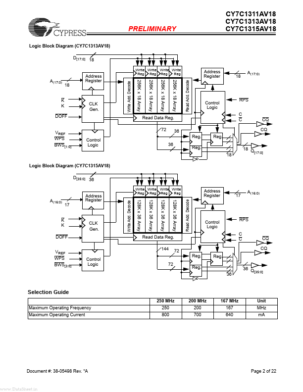
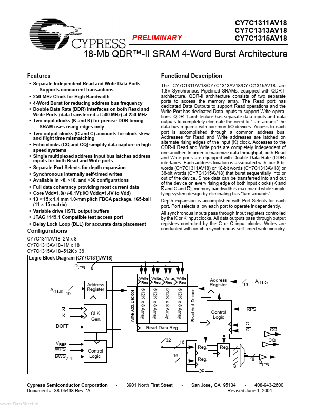
The CY7C1311AV18/CY7C1313AV18/CY7C1315AV18 are 1.8V Synchronous Pipelined SRAMs, equipped with QDR-II architecture.
QDR-II architecture consists of two separate ports to access the memory array.
| Part number | CY7C1315AV18 |
|---|---|
| Manufacturer | Cypress (Infineon) |
| File Size | 356.67 KB |
| Description | (CY7C131xAV18) 18-Mb QDRTM-II SRAM 4-Word Burst Architecture |
| Datasheet |
CY7C1315AV18 Datasheet
|
|
|
|
| Part Number | Description | Manufacturer |
|---|---|---|
| CY7C131AE | 1K/2K x 8 Dual-Port Static RAM | Cypress |
| CY7C131E | 1K/2K x 8 Dual-Port Static RAM | Cypress |
| CY7C136AE | 1K/2K x 8 Dual-Port Static RAM | Cypress |
| CY7C136E | 1K/2K x 8 Dual-Port Static RAM | Cypress |
| CY7C1370C | 512K x 36/1M x 18 Pipelined SRAM with NoBL Architecture | Cypress |
| Part Number | Description |
|---|---|
| CY7C1315BV18 | (CY7C1x1xBV18) 18-Mb QDRTM-II SRAM 4-Word Burst Architecture |
| CY7C1315CV18 | (CY7C1x1xCV18) 18-Mb QDRTM-II SRAM 4-Word Burst Architecture |
| CY7C1315JV18 | (CY7C1x1xJV18) 18-Mbit QDR II SRAM 4-Word Burst Architecture |
| CY7C1315KV18 | 18-Mbit QDR II SRAM Four-Word Burst Architecture |
| CY7C131 | 1K x 8 Dual-Port Static RAM |
The following content is an automatically extracted verbatim text from the original manufacturer datasheet and is provided for reference purposes only.