Click to expand full text
CY7C1303BV25
18-Mbit Burst of Two-Pipelined SRAM with QDR® Architecture
18-Mbit Burst of Two-Pipelined SRAM with QDR® Architecture
Features
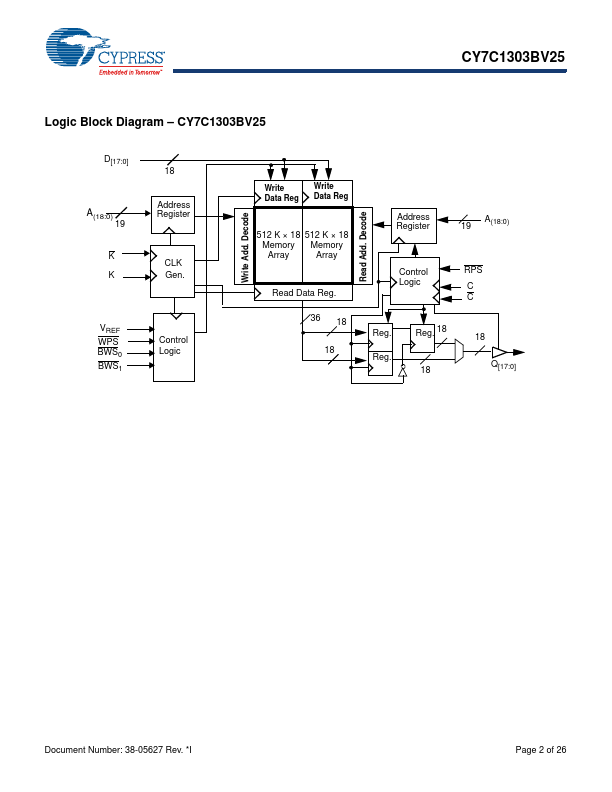
■ Separate independent read and write data ports ❐ Supports concurrent transactions
■ 167 MHz clock for high bandwidth ❐ 2.5 ns clock-to-valid access time
■ Two word burst on all accesses ■ Double data rate (DDR) interfaces on both read and write ports
(data transferred at 333 MHz) at 167 MHz ■ Two input clocks (K and K) for precise DDR timing
❐ SRAM uses rising edges only ■ Two input clocks for output data (C and C) to minimize clock
skew and flight time mismatches. ■ Single multiplexed address input bus latches address inputs
for both read and write ports ■ Separate port selects for depth expansion ■ Synchronous internally self-timed writes ■ 2.
 CY7C1303BV25 Datasheet