Datasheet Details
| Part number | CY7C1265V18 |
|---|---|
| Manufacturer | Cypress (Infineon) |
| File Size | 404.82 KB |
| Description | 1.8V Synchronous Pipelined SRAM |
| Datasheet |
 CY7C1265V18 Datasheet CY7C1265V18 Datasheet
|
|
|
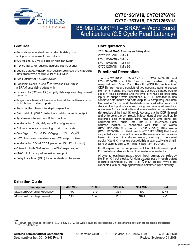
Download the CY7C1265V18 datasheet PDF. This datasheet also covers the CY7C1261V18 variant, as both devices belong to the same 1.8v synchronous pipelined sram family and are provided as variant models within a single manufacturer datasheet.
| Part number | CY7C1265V18 |
|---|---|
| Manufacturer | Cypress (Infineon) |
| File Size | 404.82 KB |
| Description | 1.8V Synchronous Pipelined SRAM |
| Datasheet |
CY7C1265V18 Datasheet
|
|
|
|
| Part Number | Description | Manufacturer |
|---|---|---|
| CY7C1006D | 1-Mbit (256K x 4) Static RAM | Cypress |
| CY7C1011G | 2-Mbit (128K words x 16 bit) Static RAM | Cypress |
| CY7C1041G | 4-Mbit (256K words x 16 bit) Static RAM | Cypress |
| CY7C1041GE | 4-Mbit (256K words x 16 bit) Static RAM | Cypress |
| CY7C1041GN | 4-Mbit (256K words x 16 bit) Static RAM | Cypress |
| Part Number | Description |
|---|---|
| CY7C1265KV18 | 36-Mbit QDR II+ SRAM Four-Word Burst Architecture |
| CY7C1265XV18 | 36-Mbit QDR II+ Xtreme SRAM Four-Word Burst Architecture |
| CY7C1261V18 | 1.8V Synchronous Pipelined SRAM |
| CY7C1262XV18 | 36-Mbit QDR II+ Xtreme SRAM Two-Word Burst Architecture |
| CY7C1263KV18 | 36-Mbit QDR II+ SRAM Four-Word Burst Architecture |