The following content is an automatically extracted verbatim text
from the original manufacturer datasheet and is provided for reference purposes only.
View original datasheet text
CY7C1263KV18/CY7C1265KV18
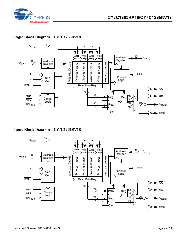
36-Mbit QDR® II+ SRAM Four-Word Burst Architecture (2.5 Cycle Read Latency)
36-Mbit QDR® II+ SRAM Four-Word Burst Architecture (2.5 Cycle Read Latency)
Features
■ Separate independent read and write data ports ❐ Supports concurrent transactions
■ 550 MHz clock for high bandwidth ■ Four-word burst for reducing address bus frequency ■ Double data rate (DDR) Interfaces on both read and write ports
(data transferred at 1100 MHz) at 550 MHz ■ Available in 2.
 CY7C1263KV18 Datasheet