Datasheet4U Logo Datasheet4U.com

CY7C1022 - 32K x 16 Static RAM

Description

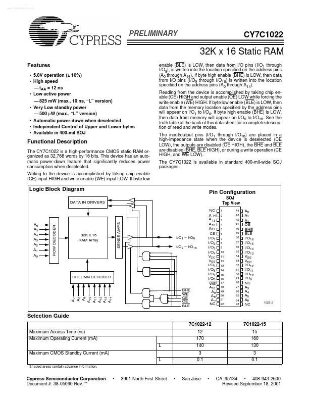
of read and write modes.

The input/output pins (I/O1 through I/O16) are placed in a high-impedance state when the device is deselected (CE LOW), the outputs are disabled (OE HIGH), the BHE and BLE are disabled (BHE, BLE HIGH), or during a write operation (CE HIGH, and WE LOW).

Features

  • 5.0V operation (± 10%).
  • High speed.
  • tAA = 12 ns.
  • Low active power.
  • 825 mW (max. , 10 ns, “L” version).
  • Very Low standby power.
  • 500 µW (max. , “L” version).
  • Automatic power-down when deselected.
  • Independent Control of Upper and Lower bytes.
  • Available in 400-mil SOJ enable (BLE) is LOW, then data from I/O pins (I/O1 through I/O8), is written into the location specified on the address pins (A0 through A14). If.

📥 Download Datasheet

Full PDF Text Transcription (Reference)

The following content is an automatically extracted verbatim text from the original manufacturer datasheet and is provided for reference purposes only.

View original datasheet text
022CY7C10 www.DataSheet4U.com PRELIMINARY CY7C1022 32K x 16 Static RAM Features • 5.0V operation (± 10%) • High speed — tAA = 12 ns • Low active power — 825 mW (max., 10 ns, “L” version) • Very Low standby power — 500 µW (max., “L” version) • Automatic power-down when deselected • Independent Control of Upper and Lower bytes • Available in 400-mil SOJ enable (BLE) is LOW, then data from I/O pins (I/O1 through I/O8), is written into the location specified on the address pins (A0 through A14). If byte high enable (BHE) is LOW, then data from I/O pins (I/O9 through I/O16) is written into the location specified on the address pins (A0 through A14). Reading from the device is accomplished by taking chip enable (CE) HIGH and output enable (OE) LOW while forcing the write enable (WE) HIGH.
Published: |