Click to expand full text
PRELIMINARY CY29351
2.5V or 3.3V, 200 MHz, 9-Output Zero Delay
Features
■ ■ ■ ■
Functional Description
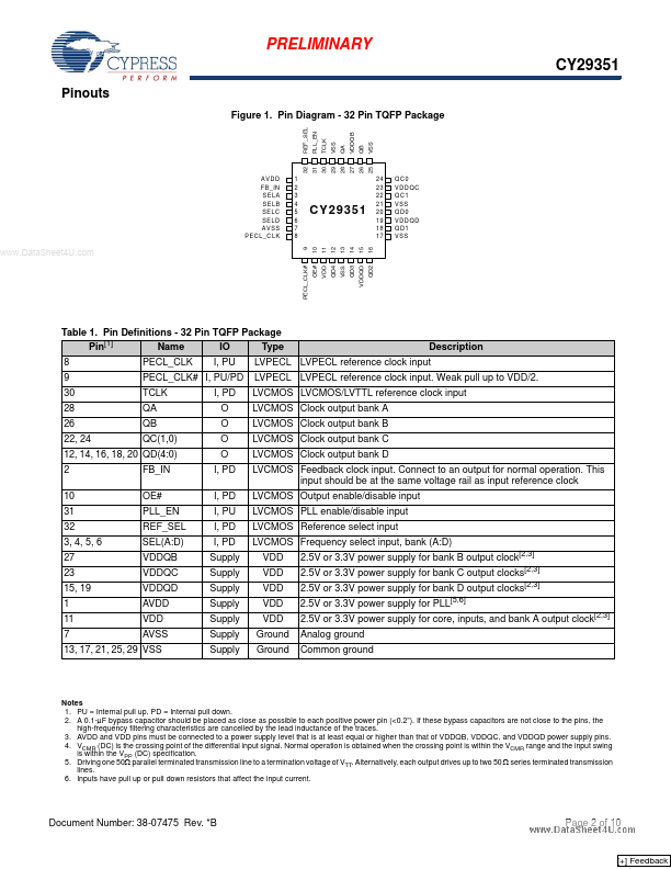
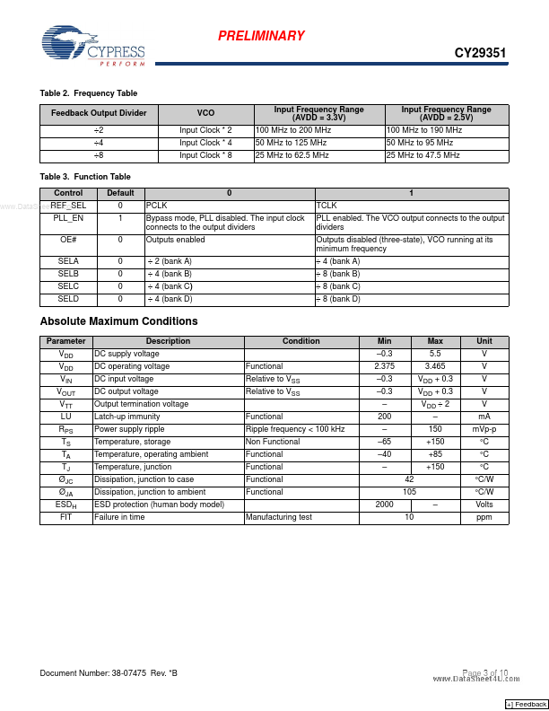
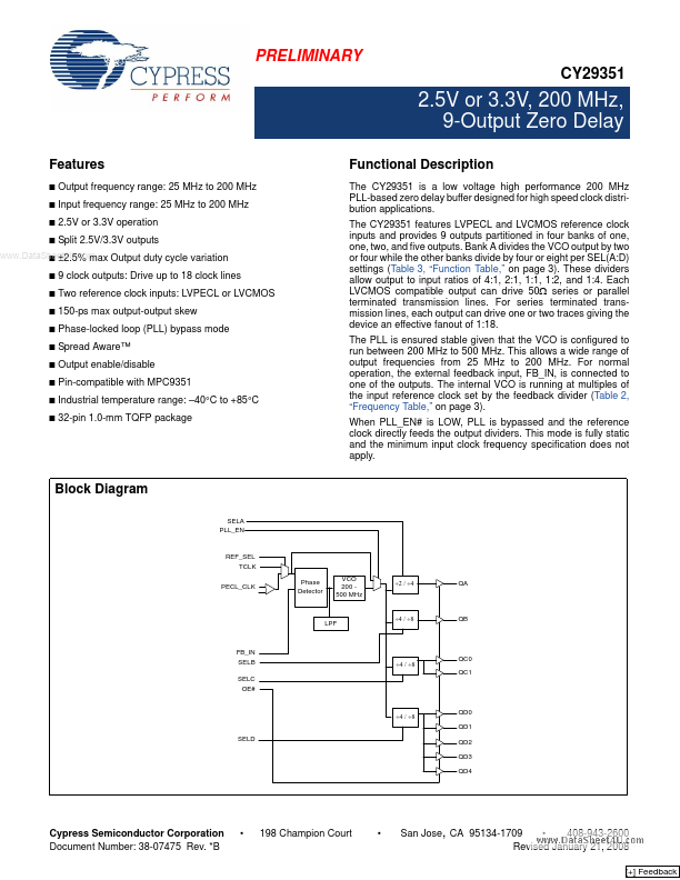
The CY29351 is a low voltage high performance 200 MHz PLL-based zero delay buffer designed for high speed clock distribution applications. The CY29351 features LVPECL and LVCMOS reference clock inputs and provides 9 outputs partitioned in four banks of one, one, two, and five outputs. Bank A divides the VCO output by two or four while the other banks divide by four or eight per SEL(A:D) settings (Table 3, “Function Table,” on page 3). These dividers allow output to input ratios of 4:1, 2:1, 1:1, 1:2, and 1:4. Each LVCMOS compatible output can drive 50Ω series or parallel terminated transmission lines.
 CY29351 Datasheet