Datasheet4U Logo Datasheet4U.com

CY28341 - Universal Single-Chip Clock Solution

Description

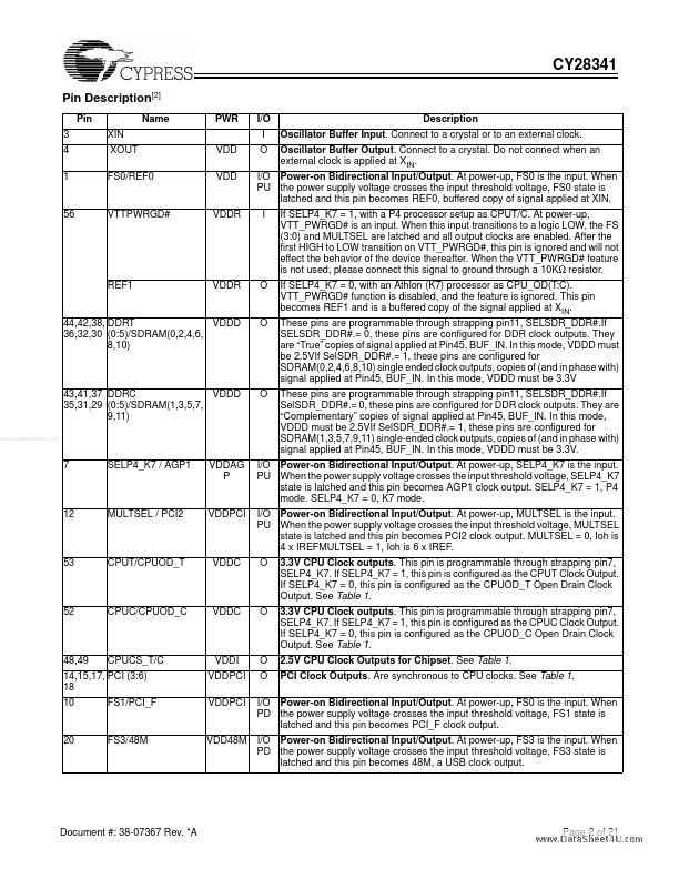
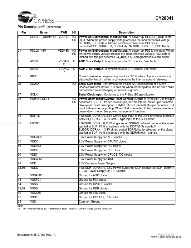
Pin 3 4 1 XIN XOUT FS0/REF0 VDD VDD Name PWR I/O I O Description Oscillator Buffer Input.

Connect to a crystal or to an external clock.

Oscillator Buffer Output.

Features

  • Supports VIA P4M266/KM266 chipsets Supports Pentium® 4, Athlon™ processors Supports two DDR DIMMS Supports three SDRAMS DIMMS at 100 MHz Provides:.
  • Two different programmable CPU clock pairs.
  • Six differential SDRAM DDR pairs.
  • Three low-skew/low-jitter AGP clocks.
  • Seven low-skew/low-jitter PCI clocks.
  • One 48M output for USB.
  • One programmable 24M or 48M for SIO.
  • Dial-a-Frequency™ and D.

📥 Download Datasheet

Datasheet preview – CY28341

Datasheet Details

Part number CY28341
Manufacturer Cypress (now Infineon)
File Size 238.03 KB
Description Universal Single-Chip Clock Solution
Datasheet download datasheet CY28341 Datasheet
Additional preview pages of the CY28341 datasheet.
Other Datasheets by Cypress Semiconductor

Full PDF Text Transcription

Click to expand full text
CY28341 Universal Single-Chip Clock Solution for VIA P4M266/KM266 DDR Systems Features • • • • • Supports VIA P4M266/KM266 chipsets Supports Pentium® 4, Athlon™ processors Supports two DDR DIMMS Supports three SDRAMS DIMMS at 100 MHz Provides: — Two different programmable CPU clock pairs — Six differential SDRAM DDR pairs — Three low-skew/low-jitter AGP clocks — Seven low-skew/low-jitter PCI clocks — One 48M output for USB — One programmable 24M or 48M for SIO • Dial-a-Frequency™ and Dial-a-dB features • Spread Spectrum for best electromagnetic interference (EMI) reduction • Watchdog feature for systems recovery • SMBus-compatible for programmability • 56-pin SSOP and TSSOP packages Table 1.
Published: |