The following content is an automatically extracted verbatim text
from the original manufacturer datasheet and is provided for reference purposes only.
View original datasheet text
CY26200
T1/E1 Clock Generator
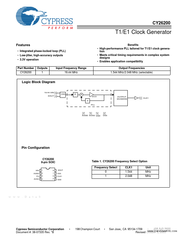
Features
• Integrated phase-locked loop (PLL) • Low-jitter, high-accuracy outputs • 3.3V operation Part Number CY26200 Outputs 1 Input Frequency Range 19.44 MHz Benefits • High-performance PLL tailored for T1/E1 clock generation • Meets critical timing requirements in complex system designs • Enables application compatibility Output Frequencies 1.544 MHz/2.048 MHz (selectable)
Logic Block Diagram
19.44 XIN XOUT
OSC
Q
Φ VCO P PLL OUTPUT DIVIDERS CLK1
AVDD AVSS VDD
VSS
Pin Configuration
CY26200 8-pin SOIC
XIN AVDD FS AVSS 1 2 3 4 8 7 6 5 XOUT VSS CLK1 VDD
Table 1. CY26200 Frequency Select Option Frequency Select 0 1 CLK1 1.544 2.048 Unit MHz MHz
w w w . D a t a S h e e t 4 U . c o m
Cypress Semiconductor Corporation Document #: 38-07335 Rev.
 CY26200 Datasheet