CEM9935A
FEATURES
20V, 6.0A, RDS(ON) = 36mΩ @VGS = 10V. RDS(ON) = 42mΩ @VGS = 4.5V. RDS(ON) = 75mΩ @VGS = 2.5V.
Super high dense cell design for extremely low RDS(ON). High power and current handing capability. Lead free product is acquired. Surface mount Package.
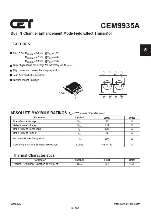
D1 D1 D2 D2 876 5
SO-8
123 4 S1 G1 S2 G2
ABSOLUTE MAXIMUM RATINGS TA = 25 C unless otherwise noted
Parameter
Symbol
Limit
Drain-Source Voltage Gate-Source Voltage
VDS 20
VGS ±12
Drain Current-Continuous Drain Current-Pulsed a
ID 6.0 IDM 24
Maximum Power Dissipation
PD 2.0
Operating and Store Temperature Range
TJ,Tstg
-55 to 150
Thermal Characteristics
Parameter Thermal Resistance, Junction-to-Ambient b
Symbol RθJA
Limit 62.5
Units V V A A W C
Units C/W
2003.July
- 233 http://.cet-mos.
Electrical Characteristics TA = 25 C unless otherwise noted
Parameter Off Characteristics Drain-Source Breakdown Voltage Zero Gate Voltage Drain Current Gate Body Leakage Current On Characteristics...