Datasheet4U Logo Datasheet4U.com

HMC987LP5E - LOW NOISE 1:9 FANOUT BUFFER

Description

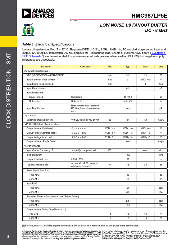
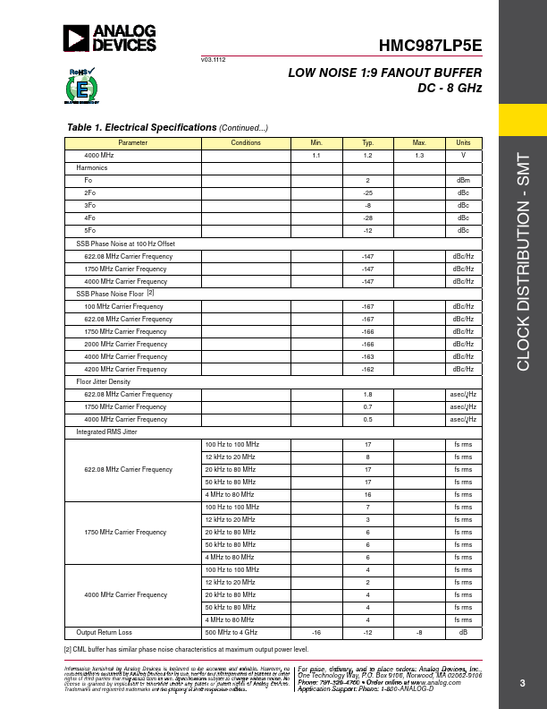
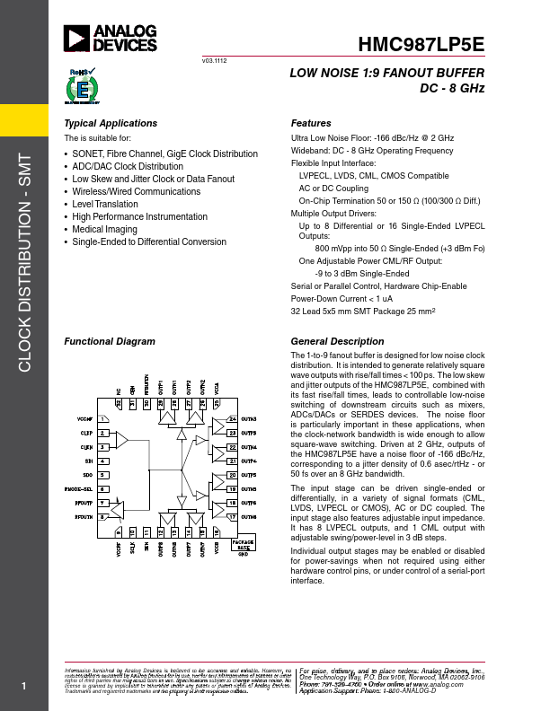
The 1-to-9 fanout buffer is designed for low noise clock distribution.

It is intended to generate relatively square wave outputs with rise/fall times < 100 ps.

Features

  • Ultra Low Noise Floor: -166 dBc/Hz @ 2 GHz Wideband: DC - 8 GHz Operating Frequency Flexible Input Interface: LVPECL, LVDS, CML, CMOS Compatible AC or DC Coupling On-Chip Termination 50 or 150 Ω (100/300 Ω Diff. ) Multiple Output Drivers: Up to 8 Differential or 16 Single-Ended LVPECL Outputs: 800 mVpp into 50 Ω Single-Ended (+3 dBm Fo) One Adjustable Power CML/RF Output: -9 to 3 dBm Single-Ended Serial or Parallel Control, Hardware Chip-Enable Power-Down Current < 1 uA 32 Lead 5x5 mm SMT Package.

📥 Download Datasheet

Datasheet preview – HMC987LP5E

Datasheet Details

Part number HMC987LP5E
Manufacturer Analog Devices
File Size 1.64 MB
Description LOW NOISE 1:9 FANOUT BUFFER
Datasheet download datasheet HMC987LP5E Datasheet
Additional preview pages of the HMC987LP5E datasheet.
Other Datasheets by Analog Devices

Full PDF Text Transcription

Click to expand full text
Clock Distribution - SMT v03.1112 Typical Applications The is suitable for: • SONET, Fibre Channel, GigE Clock Distribution • ADC/DAC Clock Distribution • Low Skew and Jitter Clock or Data Fanout • Wireless/Wired Communications • Level Translation • High Performance Instrumentation • Medical Imaging • Single-Ended to Differential Conversion Functional Diagram HMC987LP5E LOW NOISE 1:9 FANOUT BUFFER DC - 8 GHz Features Ultra Low Noise Floor: -166 dBc/Hz @ 2 GHz Wideband: DC - 8 GHz Operating Frequency Flexible Input Interface: LVPECL, LVDS, CML, CMOS Compatible AC or DC Coupling On-Chip Termination 50 or 150 Ω (100/300 Ω Diff.
Published: |