Datasheet Details
| Part number | AOD413 |
|---|---|
| Manufacturer | Alpha & Omega Semiconductors |
| File Size | 144.99 KB |
| Description | P-Channel MOSFET |
| Datasheet |
 AOD413 Datasheet AOD413 Datasheet
|
|
|
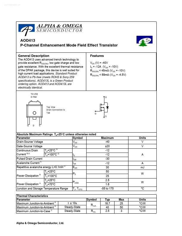
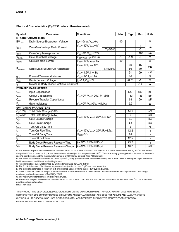
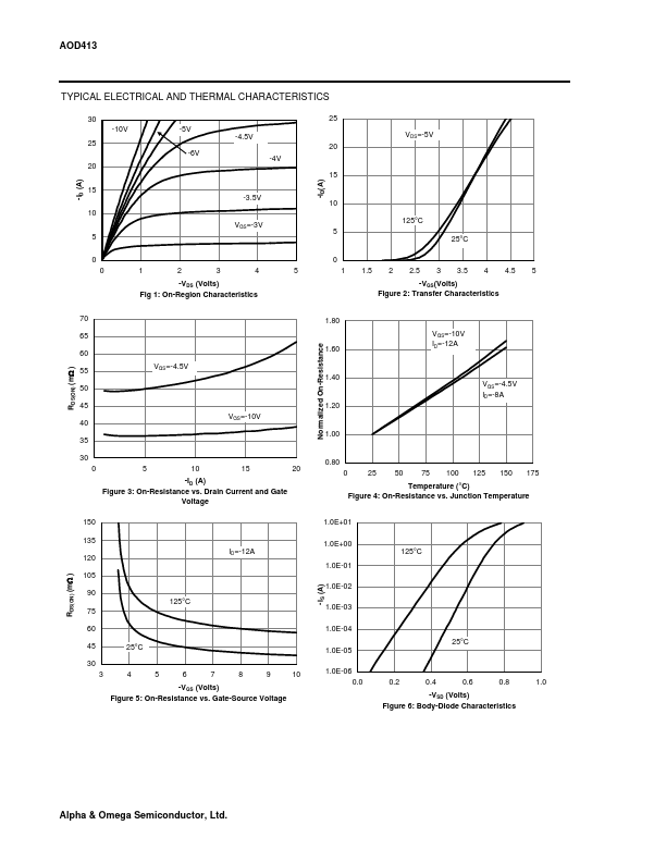
The AOD413 uses advanced trench technology to provide excellent RDS(ON), low gate charge and low gate resistance.
With the excellent thermal resistance of the DPAK package, this device is well suited for high current load applications.
| Part number | AOD413 |
|---|---|
| Manufacturer | Alpha & Omega Semiconductors |
| File Size | 144.99 KB |
| Description | P-Channel MOSFET |
| Datasheet |
AOD413 Datasheet
|
|
|
|
Note: Below is a high-fidelity text extraction (approx. 800 characters) for AOD413. For precise diagrams, and layout, please refer to the original PDF.
www.DataSheet4U.com AOD413 P-Channel Enhancement Mode Field Effect Transistor General Description The AOD413 uses advanced trench technology to provide excellent RDS(ON),...
| Brand Logo | Part Number | Description | Manufacturer |
|---|---|---|---|
| AOD413 | P-Channel MOSFET | Kexin | |
| AOD4130 | N-Channel MOSFET | INCHANGE | |
| AOD4132 | N-Channel MOSFET | INCHANGE | |
| AOD4136 | N-Channel MOSFET | INCHANGE | |
| AOD413A | N-Channel MOSFET | INCHANGE |
| Part Number | Description |
|---|---|
| AOD4130 | 60V N-Channel MOSFET |
| AOD4132 | 30v N-Channel MOSFET |
| AOD4136 | POWER Transistor |
| AOD413A | 40V P-Channel MOSFET |
| AOD413Y | P-Channel MOSFET |
| AOD410 | N-Channel MOSFET |
| AOD4100 | N-Channel MOSFET |
| AOD4102 | 30V N-Channel MOSFET |
| AOD4104 | N-Channel MOSFET |
| AOD4106 | N-Channel MOSFET |