AO3416
Description
Product Summary
The AO3416 uses advanced trench technology to provide excellent RDS(ON), low gate charge and operation with gate voltages as low as 1.8V. This device is suitable for use as a load switch or in PWM applications. It is ESD protected.
VDS ID (at VGS=4.5V) RDS(ON) (at VGS=4.5V) RDS(ON) (at VGS = 2.5V) RDS(ON) (at VGS = 1.8V)
ESD protected
20V 6.5A < 22m W < 26m W < 34m W
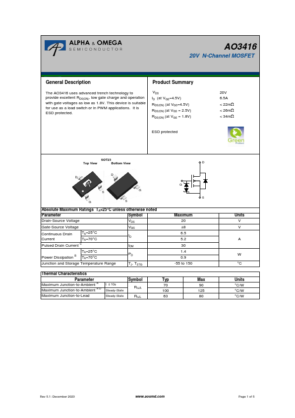
SOT23
Top View
Bottom View
Absolute Maximum Ratings TA=25°C unless otherwise noted
Parameter
Symbol
Drain-Source Voltage
Gate-Source Voltage
Continuous Drain Current
TA=25°C TA=70°C
Pulsed Drain Current C
TA=25°C Power Dissipation B TA=70°C
Junction and Storage Temperature Range
TJ, TSTG
Maximum 20 ±8 6.5 5.2 30 1.4 0.9
-55 to 150
Thermal Characteristics
Parameter
Symbol
Typ
Maximum Junction-to-Ambient A t ≤ 10s Maximum Junction-to-Ambient A D Steady-State
Rq JA
70 100
Maximum Junction-to-Lead
Steady-State
Rq...