AS7C256L
FEATURES
- Organization: 32,768 words × 8 bits
- High speed
- 10/12/15/20/25/35 ns address access time
- 3/3/4/5/6/8 ns output enable access time
- Low power consumption
- Active: 660 m W max (10 ns cycle)
- Standby: 11 m W max, CMOS I/O 2.75 m W max, CMOS I/O, L version
- Very low DC ponent in active power
- 2.0V data retention (L version)
- Equal access and cycle times
- Easy memory expansion with CE and OE inputs
- TTL-patible, three-state I/O
- 28-pin JEDEC standard packages
- 300 mil PDIP and SOJ Socket patible with 7C512 and 7C1024
- 330 mil SOIC
- 8×13.4 TSOP
- ESD protection > 2000 volts
- Latch-up current > 200 m A
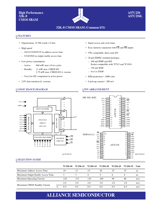
LOGIC BLOCK DIAGRAM
PIN ARRANGEMENT
ROW DECODER SENSE AMP
AS7C256
Vcc
A0 A1 A2 A3 A4 A5 A6 A14
INPUT BUFFER
256×128×8 ARRAY (262,144)
I/O7 I/O0
COLUMN DECODER
AAAAAAA 7 8 9 10 11 12 13
CONTROL CIRCUIT
WE OE CE
SELECTION...