AS7C256A
Features
- Pin patible with AS7C256
- Industrial and mercial temperature options
- Organization: 32,768 words × 8 bits
- High speed
- 10/12/15/20 ns address access time
- 5, 6, 7, 8 ns output enable access time
- Very low power consumption: ACTIVE
- 412.5 m W max @ 10 ns
- Very low power consumption: STANDBY
- 11 m W max CMOS I/O
- Easy memory expansion with CE and OE inputs
- TTL-patible, three-state I/O
- 28-pin JEDEC standard packages
- 300 mil SOJ
- 8 × 13.4 mm TSOP 1
- ESD protection ≥ 2000 volts
- Latch-up current ≥ 200 m A
- 2.0V Data retention
Row decoder Sense amp AS7C256A
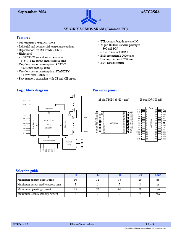
Logic block diagram
A0 A1 A2 A3 A4 A5 A6 A7
Input buffer
256 X 128 X 8 Array
(262,144)
Column decoder
AAAAAAA 8 9 10 11 12 13 14
Control circuit
Pin arrangement
28-pin TSOP 1 (8×13.4 mm)
28-pin SOJ (300 mil)
I/O7
I/O0 WE OE CE
A14
OE 1
28 A10 A12
A11 2 A9 3 A8 4
27 26...