Datasheet Details
| Part number | 74LVC4066-Q100 |
|---|---|
| Manufacturer | Nexperia |
| File Size | 296.71 KB |
| Description | Quad bilateral switch |
| Datasheet |
 74LVC4066-Q100 Datasheet 74LVC4066-Q100 Datasheet
|
|
|
The 74LVC4066-Q100 is a high-speed Si-gate CMOS device.
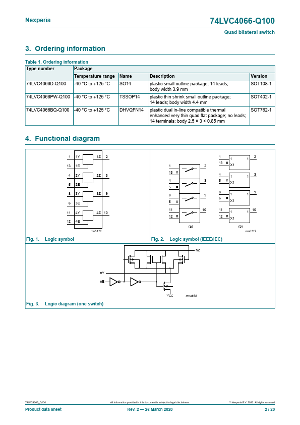
The 74LVC4066-Q100 provides four single pole, single-throw analog switch functions.
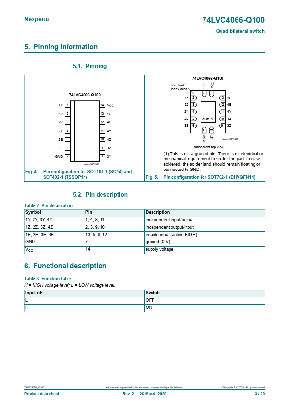
Each switch has two input/output terminals (nY and nZ) and an active HIGH enable input (nE).
| Part number | 74LVC4066-Q100 |
|---|---|
| Manufacturer | Nexperia |
| File Size | 296.71 KB |
| Description | Quad bilateral switch |
| Datasheet |
74LVC4066-Q100 Datasheet
|
|
|
|
| Part Number | Description | Manufacturer |
|---|---|---|
| 74LVC4066 | Quad bilateral switches | NXP |
| 74LVC4245A | Octal dual supply translating transceiver | NXP |
| 74LVC00A | LOW VOLTAGE CMOS QUAD 2-INPUT NAND GATE | STMicroelectronics |
| 74LVC00A | QUADRUPLE 2-INPUT NAND GATES | Diodes |
| 74LVC00A | Low-Voltage CMOS Quad 2-Input NAND Gate | ON Semiconductor |
| Part Number | Description |
|---|---|
| 74LVC4066 | Quad bilateral switch |
| 74LVC4245A | Octal dual supply translating transceiver |
| 74LVC4245A-Q100 | Octal dual supply translating transceiver |
| 74LVC4245AD | Octal dual supply translating transceiver |
| 74LVC4T3144 | 4-bit dual supply buffer/line driver |
The following content is an automatically extracted verbatim text from the original manufacturer datasheet and is provided for reference purposes only.