Click to expand full text
74LVC4066
Quad bilateral switch
Rev. 6 — 26 March 2020
Product data sheet
1. General description
The 74LVC4066 is a high-speed Si-gate CMOS device.
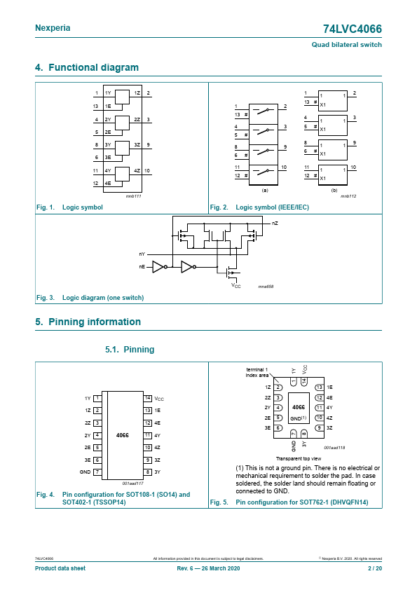
The 74LVC4066 provides four single pole, single-throw analog switch functions. Each switch has two input/output terminals (nY and nZ) and an active HIGH enable input (nE). When nE is LOW, the analog switch is turned off.
Schmitt-trigger action at the enable inputs makes the circuit tolerant of slower input rise and fall times across the entire VCC range from 1.65 V to 5.5 V.
2. Features and benefits
• Wide supply voltage range from 1.65 V to 5.5 V • Very low ON resistance:
• 7.5 Ω (typical) at VCC = 2.7 V • 6.5 Ω (typical) at VCC = 3.
 74LVC4066 Datasheet