Datasheet4U Logo Datasheet4U.com

SN74AUP1T00 - POSITIVE-NAND GATE

Description

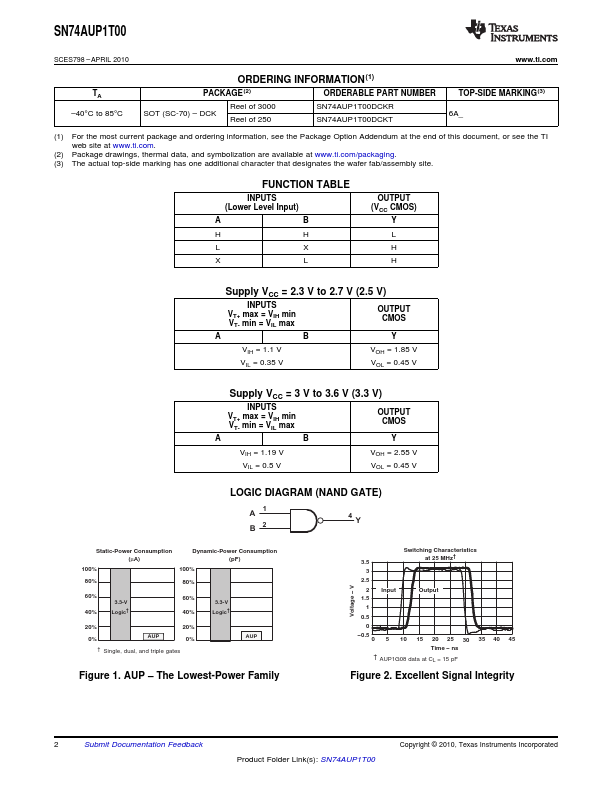
ORDERING INFORMATION 
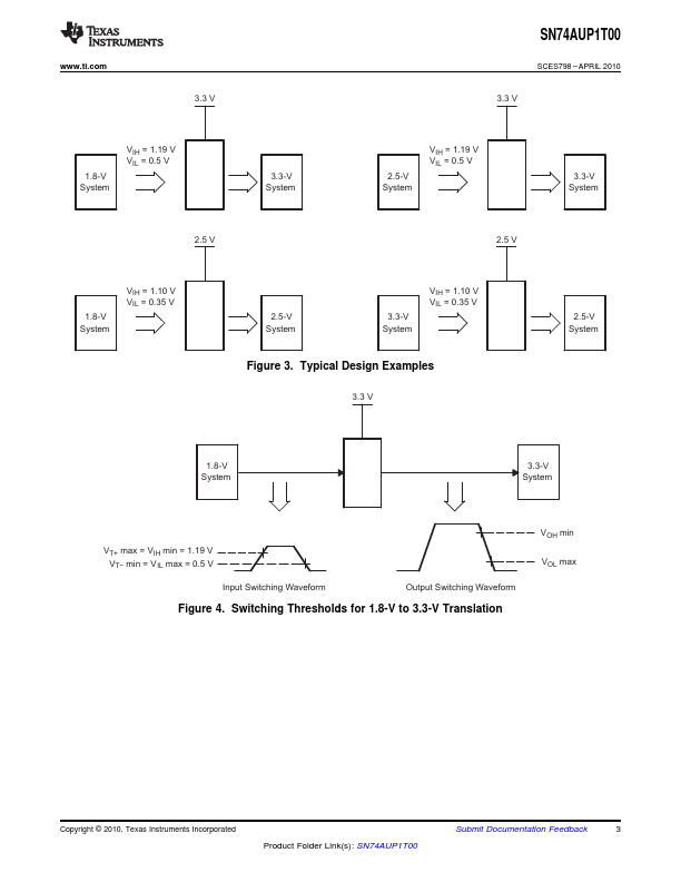
The SN74AUP1T00 performs the Boolean function Y = A

B or Y = A + B with designation for logic-level translation applications with output referenced to supply VCC.
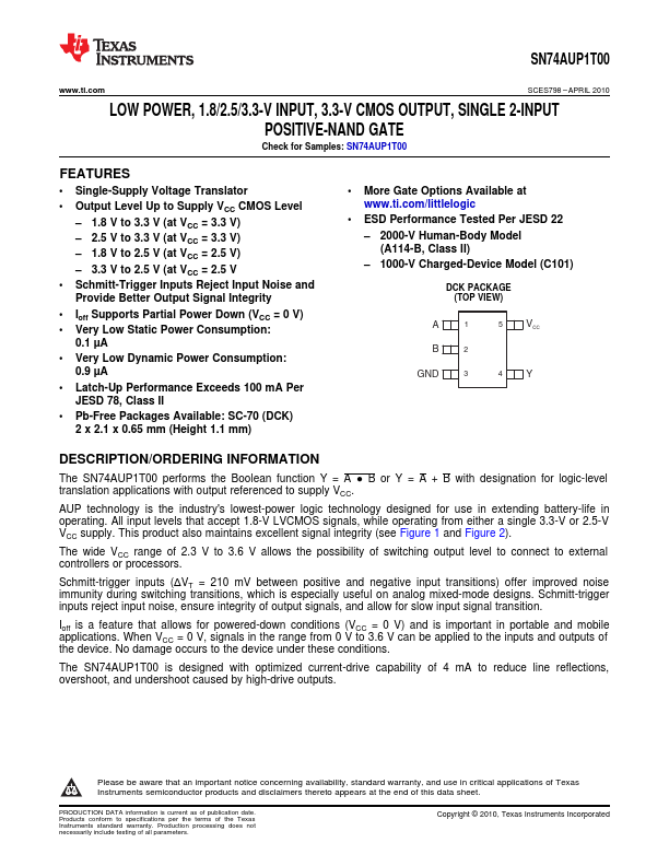
Features

  • 1.
  • Single-Supply Voltage Translator.
  • Output Level Up to Supply VCC CMOS Level.
  • 1.8 V to 3.3 V (at VCC = 3.3 V).
  • 2.5 V to 3.3 V (at VCC = 3.3 V).
  • 1.8 V to 2.5 V (at VCC = 2.5 V).
  • 3.3 V to 2.5 V (at VCC = 2.5 V.
  • Schmitt-Trigger Inputs Reject Input Noise and Provide Better Output Signal Integrity.
  • Ioff Supports Partial Power Down (VCC = 0 V).
  • Very Low Static Power Consumption: 0.1 µA.
  • Very Low Dynamic Power Co.

📥 Download Datasheet

Full PDF Text Transcription (Reference)

The following content is an automatically extracted verbatim text from the original manufacturer datasheet and is provided for reference purposes only.

View original datasheet text
SN74AUP1T00 www.ti.com SCES798 – APRIL 2010 LOW POWER, 1.8/2.5/3.3-V INPUT, 3.3-V CMOS OUTPUT, SINGLE 2-INPUT POSITIVE-NAND GATE Check for Samples: SN74AUP1T00 FEATURES 1 • Single-Supply Voltage Translator • Output Level Up to Supply VCC CMOS Level – 1.8 V to 3.3 V (at VCC = 3.3 V) – 2.5 V to 3.3 V (at VCC = 3.3 V) – 1.8 V to 2.5 V (at VCC = 2.5 V) – 3.3 V to 2.5 V (at VCC = 2.5 V • Schmitt-Trigger Inputs Reject Input Noise and Provide Better Output Signal Integrity • Ioff Supports Partial Power Down (VCC = 0 V) • Very Low Static Power Consumption: 0.1 µA • Very Low Dynamic Power Consumption: 0.9 µA • Latch-Up Performance Exceeds 100 mA Per JESD 78, Class II • Pb-Free Packages Available: SC-70 (DCK) 2 x 2.1 x 0.65 mm (Height 1.1 mm) • More Gate Options Available at www.ti.
Published: |