Click to expand full text
www.ti.com
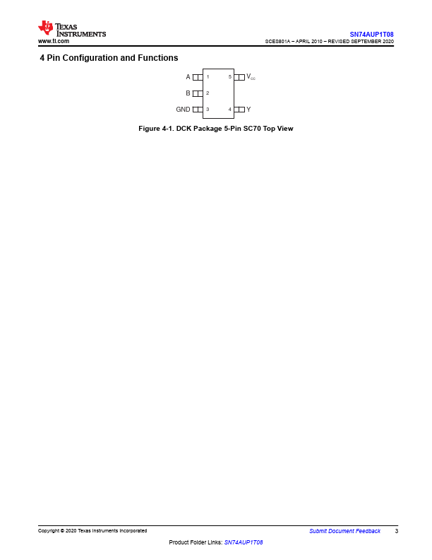
SN74AUP1T08 SCES801A – APRIL 2010 – REVISEDSSENP7T4EAMUBEPR12T00280
SCES801A – APRIL 2010 – REVISED SEPTEMBER 2020
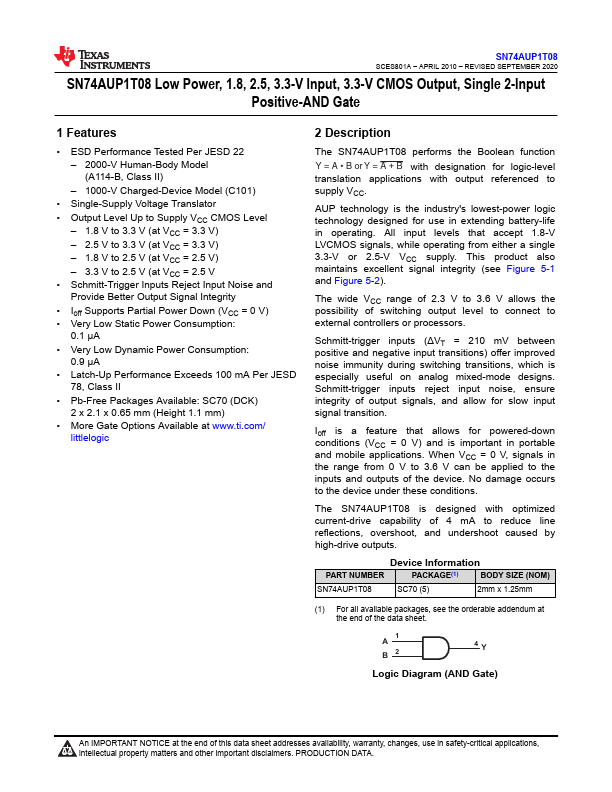
SN74AUP1T08 Low Power, 1.8, 2.5, 3.3-V Input, 3.3-V CMOS Output, Single 2-Input
Positive-AND Gate
1 Features
• ESD Performance Tested Per JESD 22
– 2000-V Human-Body Model (A114-B, Class II)
– 1000-V Charged-Device Model (C101)
• Single-Supply Voltage Translator
• Output Level Up to Supply VCC CMOS Level – 1.8 V to 3.3 V (at VCC = 3.3 V) – 2.5 V to 3.3 V (at VCC = 3.3 V) – 1.8 V to 2.5 V (at VCC = 2.5 V) – 3.3 V to 2.5 V (at VCC = 2.5 V
• Schmitt-Trigger Inputs Reject Input Noise and Provide Better Output Signal Integrity
• Ioff Supports Partial Power Down (VCC = 0 V) • Very Low Static Power Consumption:
0.1 µA
• Very Low Dynamic Power Consumption: 0.
 SN74AUP1T08 Datasheet