Datasheet Details
| Part number | CDCV855I |
|---|---|
| Manufacturer | Texas Instruments |
| File Size | 355.56 KB |
| Description | 2.5-V PHASE-LOCK LOOP CLOCK DRIVER |
| Datasheet |
 CDCV855I Datasheet CDCV855I Datasheet
|
|
|
Download the CDCV855I datasheet PDF. This datasheet also covers the CDCV855 variant, as both devices belong to the same 2.5-v phase-lock loop clock driver family and are provided as variant models within a single manufacturer datasheet.
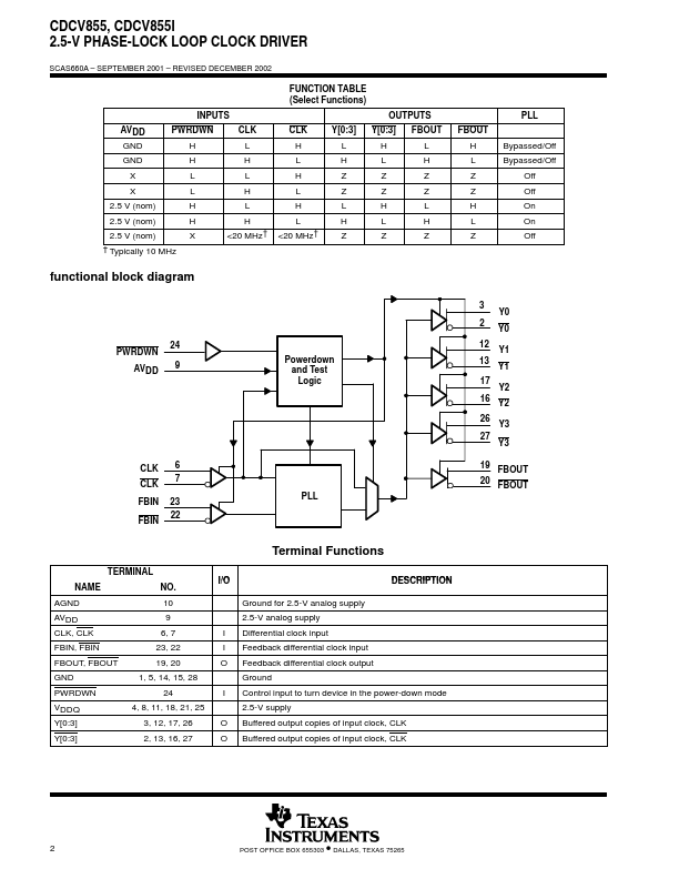
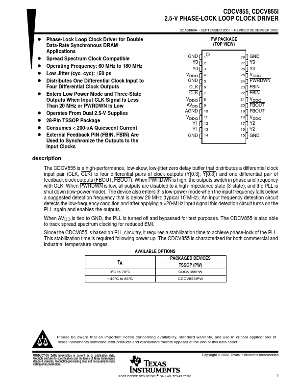
The CDCV855 is a high-performance, low-skew, low-jitter zero delay buffer that distributes a differential clock input pair (CLK, CLK) to four differential pairs of clock outputs (Y[0:3], Y[0:3]) and one differential pair of feedback clock outputs (FBOUT, FBOUT).
| Part number | CDCV855I |
|---|---|
| Manufacturer | Texas Instruments |
| File Size | 355.56 KB |
| Description | 2.5-V PHASE-LOCK LOOP CLOCK DRIVER |
| Datasheet |
CDCV855I Datasheet
|
|
|
|
| Part Number | Description | Manufacturer |
|---|---|---|
| CDC-Z137 | FM / AM CD Player | Aiwa |
| CDC1607F-E | Automotive Controller Specification | Micronas |
| CDC1631F-E | Automotive Controller | Micronas |
| CDC3207G-C | Automotive Controller | Micronas |
| CDC3207G-C3 | Automotive Controller | Micronas |
| Part Number | Description |
|---|---|
| CDCV855 | 2.5-V PHASE-LOCK LOOP CLOCK DRIVER |
| CDCV850 | 2.5-V Phase Lock Loop Clock Driver |
| CDCV850I | 2.5-V Phase Lock Loop Clock Driver |
| CDCV857A | 2.5-V PHASE LOCK LOOP CLOCK DRIVER |
| CDCV857B | 2.5-V PHASE LOCK LOOP CLOCK DRIVER |
The following content is an automatically extracted verbatim text from the original manufacturer datasheet and is provided for reference purposes only.