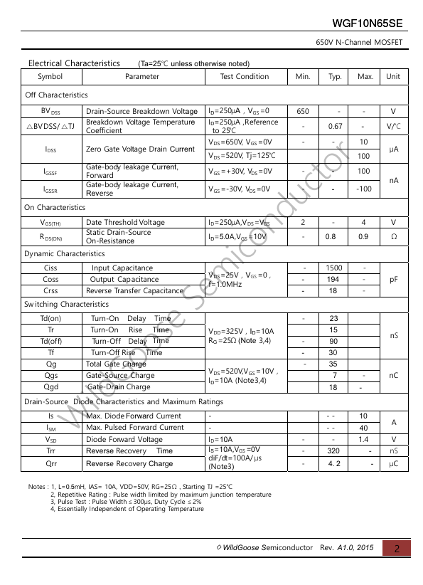
100% Avalanche Tested
D(2) G(1)
ndS(3) ico Absolute Maximum Ratings (Ta=25℃ unless otherwise noted)
1.Gate (G) 2.Drain (D) 3.Source (S)
Sy mbol VDSS
ID
VGSS E AS IAR PD Tj T stg
Drain-Source Voltage Drain Current
Sem Parameter.
The following content is an automatically extracted verbatim text
from the original manufacturer datasheet and is provided for reference purposes only.
View original datasheet text
WGF10N65SE
650V N-Channel MOSFET
TO -220F
WGF10N65SE
Features:
□ Low Intrinsic Capacitances. □ Excellent Switching Characteristics.
r □ Extended Safe Operating Area. o □ Unrivalled Gate Charge :Qg=35nC (Typ.). t □ BVDSS=650 V,ID=10A c □ RDS(on) : 0.9 Ω (Max) @VG=10V u □ 100% Avalanche Tested
D(2) G(1)
ndS(3) ico Absolute Maximum Ratings (Ta=25℃ unless otherwise noted)
1.Gate (G) 2.Drain (D) 3.Source (S)
Sy mbol VDSS
ID
VGSS E AS IAR PD Tj T stg
Drain-Source Voltage Drain Current
Sem Parameter
e Gate-Source Voltage s Single Pulse Avalanche Energy (note1) oo Avalanche Current (note2)
Power Dissipation (Tj=25℃)
G Junction Temperature(Max) ildStorage Temperature
Value
Unit
650
V
Tj=25 ℃
10
A
Tj =100℃
6.
 WGF10N65SE Datasheet