The following content is an automatically extracted verbatim text
from the original manufacturer datasheet and is provided for reference purposes only.
View original datasheet text
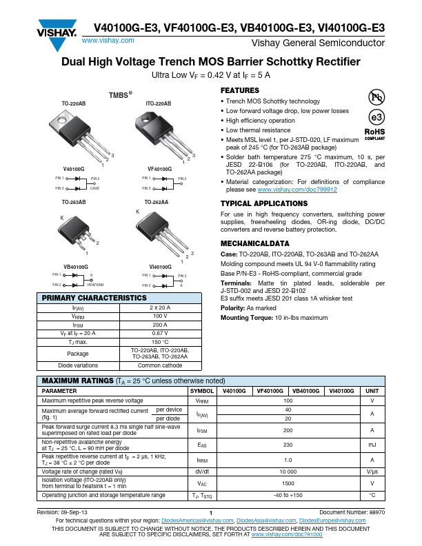
V40100G-E3, VF40100G-E3, VB40100G-E3, VI40100G-E3
www.vishay.com
Vishay General Semiconductor
Dual High Voltage Trench MOS Barrier Schottky Rectifier
Ultra Low VF = 0.42 V at IF = 5 A
TO-220AB
TMBS ®
ITO-220AB
V40100G
3 2 1
PIN 1
PIN 2
PIN 3
CASE
VF40100G
123
PIN 1
PIN 2
PIN 3
FEATURES
• Trench MOS Schottky technology
• Low forward voltage drop, low power losses
• High efficiency operation
• Low thermal resistance
• Meets MSL level 1, per J-STD-020, LF maximum peak of 245 °C (for TO-263AB package)
• Solder bath temperature 275 °C maximum, 10 s, per JESD 22-B106 (for TO-220AB, ITO-220AB, and TO-262AA package)
• Material categorization: For definitions of compliance please see www.vishay.
 V40100G-E3 Datasheet