Click to expand full text
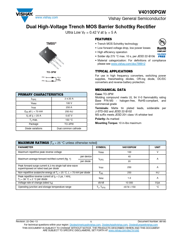
www.vishay.com
V40100PGW
Vishay General Semiconductor
Dual High-Voltage Trench MOS Barrier Schottky Rectifier
Ultra Low VF = 0.42 V at IF = 5 A
TMBS®
FEATURES • Trench MOS Schottky technology • Low forward voltage drop, low power losses • High efficiency operation • Solder dip 275 °C max. 10 s, per JESD 22-B106 • Material categorization: For definitions of compliance
please see www.vishay.com/doc?99912
TO-3PW
PIN 1 PIN 3
PIN 2 CASE
TYPICAL APPLICATIONS
For use in high frequency converters, switching power supplies, freewheeling diodes, OR-ing diode, DC/DC converters and reverse battery protection.
PRIMARY CHARACTERISTICS
IF(AV) VRRM IFSM EAS at L = 70 mH VF at IF = 20 A TJ max. Package
2 x 20 A 100 V 250 A 250 mJ 0.
 V40100PGW Datasheet