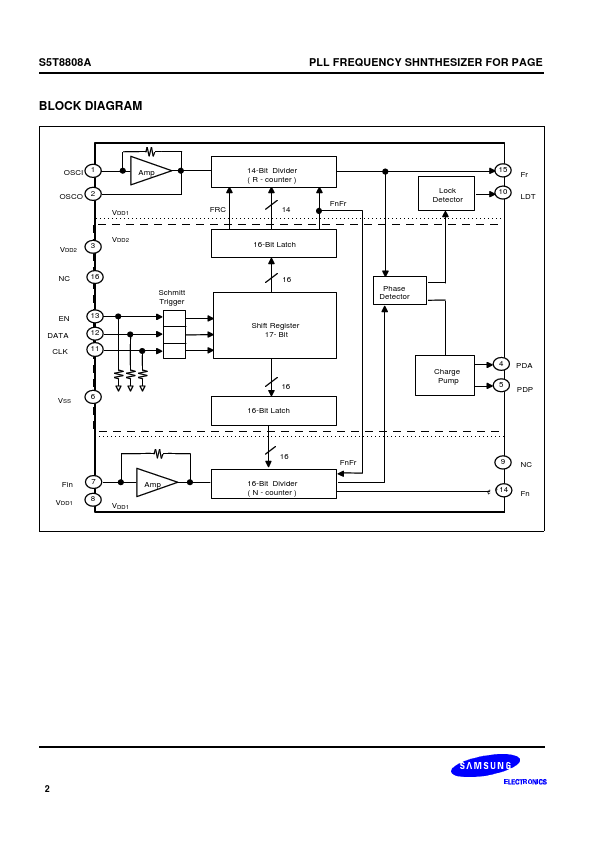
Description
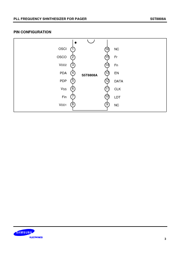
Pin No 1 2 3 4 Symbol OSCI OSCO VDD2 PDA I/O I O
O Description These input / output pins generate the reference frequency.
If Fr > Fn (Fr is leading), the output is
Features
- Maximum operating frequency: 120MHz @ 500mVP-P, VDD1 = 0.95V, VDD2 = 3.0V 165MHz @ 500mVP-P, VDD1 = 1.0V, VDD2 = 3.0V
( Magnification = 1 : 4 ).
- On-chip reference oscillator supports external crystal which oscillates up to 18MHz Superior supply current: FFIN = 90MHz, IDD1 = 0.6mA (Typ. ) @ VDD1 = 1.0V, VDD2 = 3.0V FFIN = 150MHz, IDD1 = 0.9mA (Typ. ) @ VDD1 = 1.0V, VDD2 = 3.0V Operating voltage: VDD1 = 0.95 ~ 2.0V and VDD2 = 2.0 ~ 3.3V Reference frequency counter div.
 S5T8808A_Samsungsemiconductor.pdf