Datasheet4U Logo Datasheet4U.com

ICS854S296I-33 LVDS Programmable Delay-Line

ICS854S296I-33 Description

FemtoClock® LVDS Programmable Delay Line ICS854S296I-33 DATA SHEET General .
The ICS854S296I-33 is a high performance LVDS Programmable Delay Line.

ICS854S296I-33 Features

* One LVDS level output
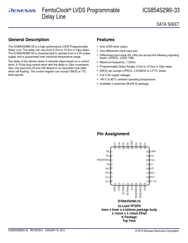
* One differential clock input pair
* Differential input clock (IN, nIN) can accept the following signaling levels: LVPECL, LVDS, CML
* Maximum frequency: 1.2GHz
* Programmable Delay Range: 2.2ns to 12.5ns in 10ps steps
* D[9:0]

📥 Download Datasheet

Preview of ICS854S296I-33 PDF
datasheet Preview Page 2 datasheet Preview Page 3

📁 Related Datasheet

  • ICS854S202I - Differential-to-LVDS Multiplexer (IDT)
  • ICS854S204I - LVPECL FANOUT BUFFER (Integrated Device Technology)
  • ICS854S006I - Differential-to-LVDS Fanout Buffer (IDT)
  • ICS854S013 - 1-TO-3 DIFFERENTIAL-TO-LVDS FANOUT BUFFER (Integrated Device Technology)
  • ICS854S057BI - 4:1 or 2:1 LVDS Clock Multiplexer (Integrated Device Technology)
  • ICS85401 - 2:1 DIFFERENTIAL-TO-LVDS MULTIPLEXER (Integrated Circuit Systems)
  • ICS854054 - 4:1 DIFFERENTIAL-TO-LVDS CLOCK MULTIPLEXER (Integrated Circuit Systems)
  • ICS854057 - 4:1 OR 2:1 LVDS CLOCK MULTIPLEXER (Integrated Circuit Systems)

📌 All Tags

Renesas ICS854S296I-33-like datasheet