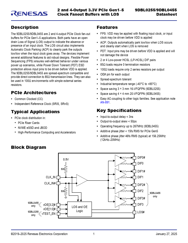
Datasheet4U Logo Datasheet4U.com

9DBL0255 - 2 and 4-Output 3.3V PCIe Gen1-5 Clock Fanout Buffers

Description

The 9DBL0255/9DBL0455 are 2 and 4-output PCIe Clock fan-out buffers for PCIe Gen1

5 applications.

Both parts have an open drain Loss of Signal (LOS) output to indicate the absence or presence of an input clock.

Features

  • to aid robust designs. Flexible Power Sequencing (FPS) ensures well-defined behavior under various power up scenarios, while Power Down Tolerant (PDT) ESD protection allows input pins to be driven before VDD is applied. The 9DBL0255/9DBL0455 are spread-spectrum compatible and provide direct connection to 85Ω transmission lines. They can also be used in 100Ω environments with simple external series resistors. PCIe Architectures.
  • Common Clocked (CC).
  • Independent Reference Clock (SRIS, SR.
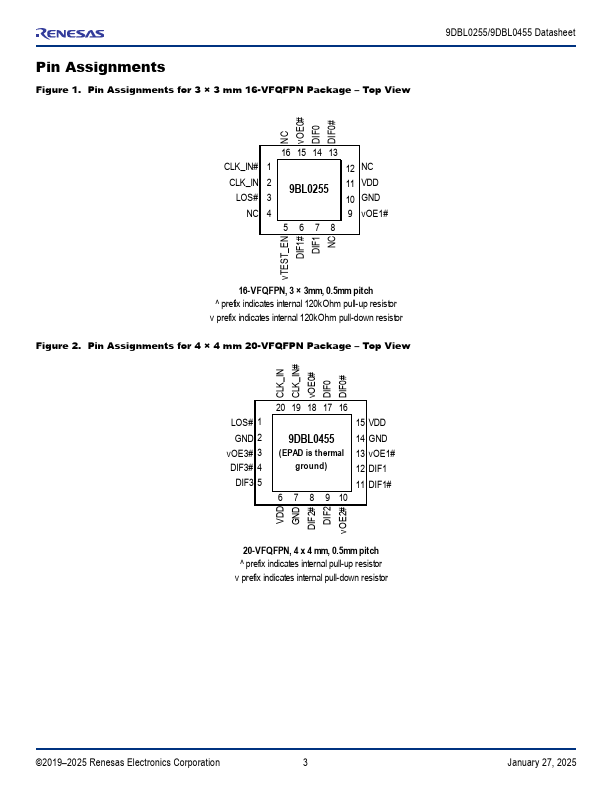
📥 Download Datasheet

Datasheet Details

Part number 9DBL0255
Manufacturer Renesas
File Size 685.23 KB
Description 2 and 4-Output 3.3V PCIe Gen1-5 Clock Fanout Buffers
Datasheet download datasheet 9DBL0255 Datasheet

Full PDF Text Transcription (Reference)

The following content is an automatically extracted verbatim text from the original manufacturer datasheet and is provided for reference purposes only.

View original datasheet text
2 and 4-Output 3.3V PCIe Gen1–5 Clock Fanout Buffers with LOS 9DBL0255/9DBL0455 Datasheet Description The 9DBL0255/9DBL0455 are 2 and 4-output PCIe Clock fan-out buffers for PCIe Gen1–5 applications. Both parts have an open drain Loss of Signal (LOS) output to indicate the absence or presence of an input clock. The LOS circuit also implements Automatic Clock Parking (ACP) to cleanly park the outputs low/low when the input clock goes away. The devices implement several additional features to aid robust designs. Flexible Power Sequencing (FPS) ensures well-defined behavior under various power up scenarios, while Power Down Tolerant (PDT) ESD protection allows input pins to be driven before VDD is applied.
Published: |