Datasheet Details
| Part number | PLL620-06 |
|---|---|
| Manufacturer | PhaseLink |
| File Size | 180.03 KB |
| Description | (PLL620-05/06/07/08/09) Low Phase Noise XO |
| Datasheet |
 PLL620-06 Datasheet PLL620-06 Datasheet
|
|
|
Download the PLL620-06 datasheet PDF. This datasheet also covers the PLL620-05 variant, as both devices belong to the same (pll620-05/06/07/08/09) low phase noise xo family and are provided as variant models within a single manufacturer datasheet.
| Part number | PLL620-06 |
|---|---|
| Manufacturer | PhaseLink |
| File Size | 180.03 KB |
| Description | (PLL620-05/06/07/08/09) Low Phase Noise XO |
| Datasheet |
PLL620-06 Datasheet
|
|
|
|
| Part Number | Description | Manufacturer |
|---|---|---|
| PLL0210A | PHASE LOCKED LOOP | Z-Communications |
| PLL0930A | PHASE LOCKED LOOP | Z-Communications |
| PLL1000A | PHASE LOCKED LOOP | Z-Communications |
| PLL102-03 | Low Skew Output Buffer | PhaseLink Corporation |
| PLL102-04 | Low Skew Output Buffer | PhaseLink Corporation |
| Part Number | Description |
|---|---|
| PLL620-00 | Low Phase Noise XO |
| PLL620-05 | (PLL620-05/06/07/08/09) Low Phase Noise XO |
| PLL620-07 | (PLL620-05/06/07/08/09) Low Phase Noise XO |
| PLL620-08 | (PLL620-05/06/07/08/09) Low Phase Noise XO |
| PLL620-09 | (PLL620-05/06/07/08/09) Low Phase Noise XO |
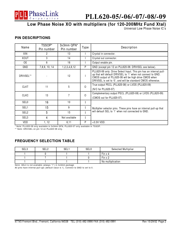
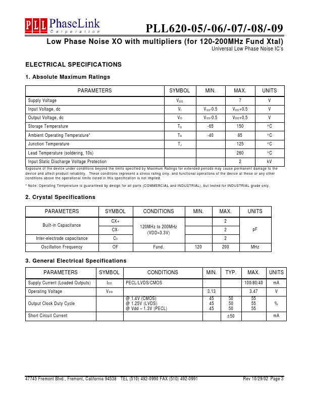
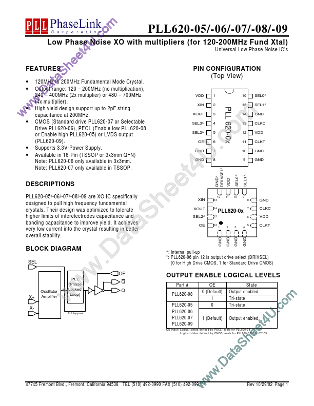
The following content is an automatically extracted verbatim text from the original manufacturer datasheet and is provided for reference purposes only.