The following content is an automatically extracted verbatim text
from the original manufacturer datasheet and is provided for reference purposes only.
View original datasheet text
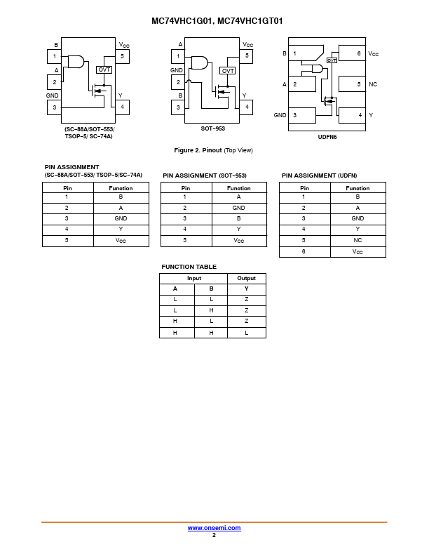
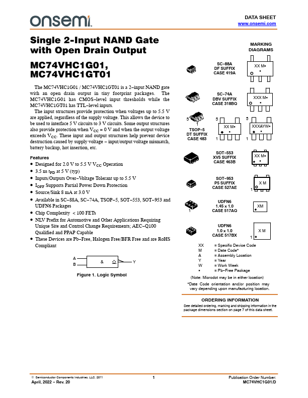
Single 2-Input NAND Gate with Open Drain Output
MC74VHC1G01, MC74VHC1GT01
The MC74VHC1G01 / MC74VHC1GT01 is a 2−input NAND gate with an open drain output in tiny footprint packages. The MC74VHC1G01 has CMOS−level input thresholds while the MC74VHC1GT01 has TTL−level inputs.
The input structures provide protection when voltages up to 5.5 V are applied, regardless of the supply voltage. This allows the device to be used to interface 5 V circuits to 3 V circuits. Some output structures also provide protection when VCC = 0 V and when the output voltage exceeds VCC. These input and output structures help prevent device destruction caused by supply voltage − input/output voltage mismatch, battery backup, hot insertion, etc.
Features
• Designed for 2.0 V to 5.5 V VCC Operation • 3.
 MC74VHC1G01 Datasheet