Full PDF Text Transcription for MC74VHC1G04 (Reference)
Note: Below is a high-fidelity text extraction (approx. 800 characters) for
MC74VHC1G04. For precise diagrams, and layout, please refer to the original PDF.
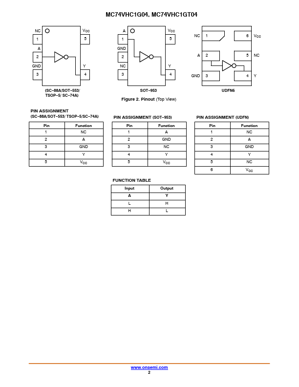
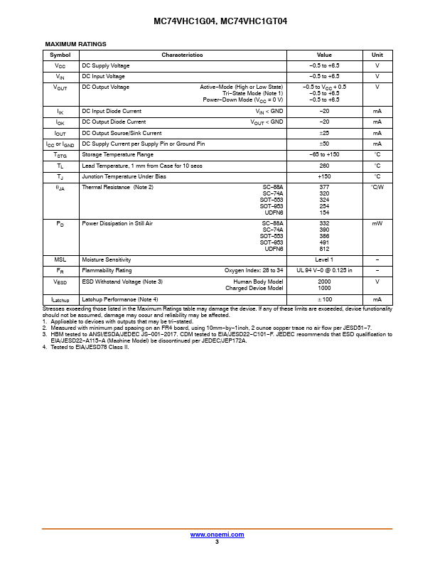
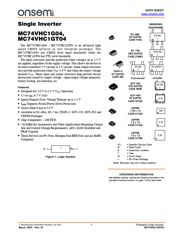
Single Inverter MC74VHC1G04, MC74VHC1GT04 The MC74VHC1G04 / MC74VHC1GT04 is an advanced high speed CMOS inverter in tiny footprint packages. The MC74VHC1G04 has CMOS leve...
View more extracted text
MOS inverter in tiny footprint packages. The MC74VHC1G04 has CMOS level input thresholds while the MC74VHC1GT04 has TTL level thresholds. The input structures provide protection when voltages up to 5.5 V are applied, regardless of the supply voltage. This allows the device to be used to interface 5 V circuits to 3 V circuits. Some output structures also provide protection when VCC = 0 V and when the output voltage exceeds VCC. These input and output structures help prevent device destruction caused by supply voltage − input/output voltage mismatch, battery backup, hot insertion, etc. Features • Designed for 2.0 V to 5.5 V
 MC74VHC1G04 Datasheet