Datasheet4U Logo Datasheet4U.com

FDPC5018SG - Dual N-Channel MOSFET

Description

a dual package.

The switch node has been internally connected to enable easy placement and routing of synchronous buck converters.

The control MOSFET (Q1) and synchronous SyncFETt (Q2) have been designed to provide optimal power efficiency.

Features

  • Q1: N-Channel.
  • Max RDS(on) = 5.0 mW at VGS = 10 V, ID = 17 A.
  • Max RDS(on) = 6.5 mW at VGS = 4.5 V, ID = 14 A Q2: N-Channel.
  • Max RDS(on) = 1.6 mW at VGS = 10 V, ID = 32 A.
  • Max RDS(on) = 2.0 mW at VGS = 4.5 V, ID = 28 A.
  • Low Inductance Packaging Shortens Rise/Fall Times, Resulting in Lower Switching Losses.
  • MOSFET Integration Enables Optimum Layout for Lower Circuit Inductance and Reduced Switch Node Ringing.
  • ESD Protection Level: HB.

📥 Download Datasheet

Datasheet Details

Part number FDPC5018SG
Manufacturer onsemi
File Size 509.67 KB
Description Dual N-Channel MOSFET
Datasheet download datasheet FDPC5018SG Datasheet

Full PDF Text Transcription

Click to expand full text
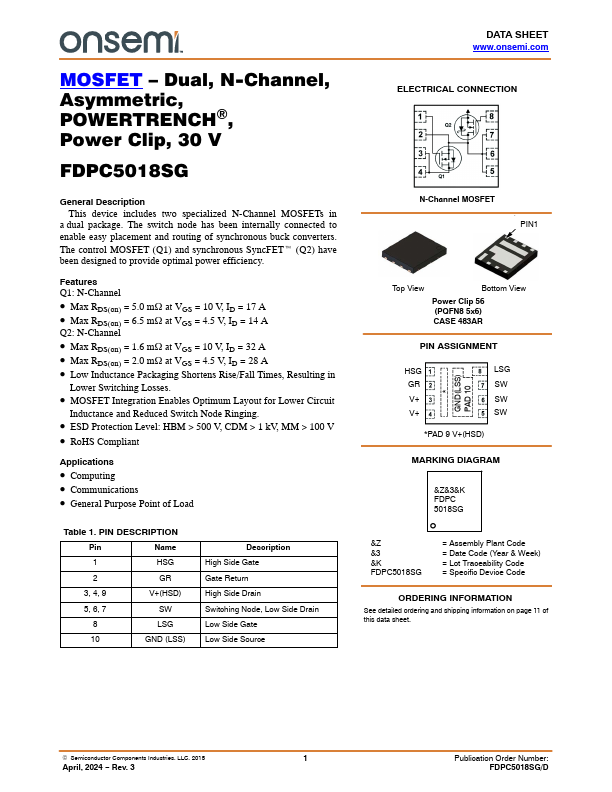
MOSFET – Dual, N-Channel, Asymmetric, POWERTRENCH), Power Clip, 30 V FDPC5018SG General Description This device includes two specialized N-Channel MOSFETs in a dual package. The switch node has been internally connected to enable easy placement and routing of synchronous buck converters. The control MOSFET (Q1) and synchronous SyncFETt (Q2) have been designed to provide optimal power efficiency. Features Q1: N-Channel • Max RDS(on) = 5.0 mW at VGS = 10 V, ID = 17 A • Max RDS(on) = 6.5 mW at VGS = 4.5 V, ID = 14 A Q2: N-Channel • Max RDS(on) = 1.6 mW at VGS = 10 V, ID = 32 A • Max RDS(on) = 2.0 mW at VGS = 4.5 V, ID = 28 A • Low Inductance Packaging Shortens Rise/Fall Times, Resulting in Lower Switching Losses.
Published: |