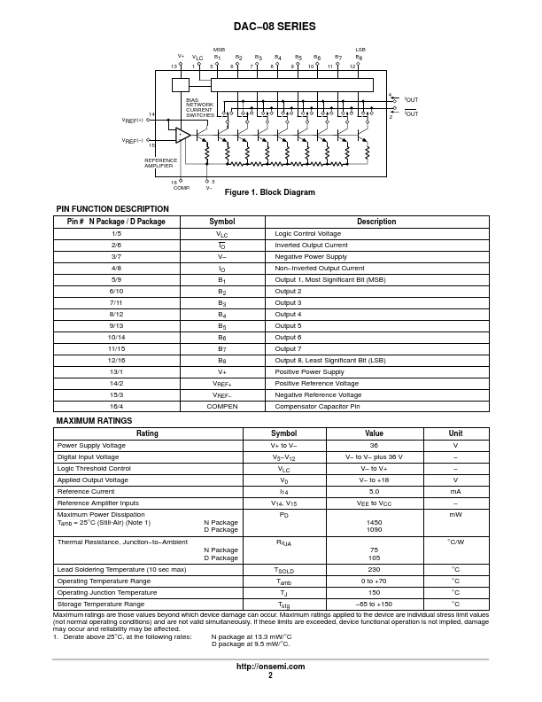
Description
Pin # N Package / D Package 1/5 2/6 3/7 4/8 5/9 6/10 7/11 8/12 9/13
10/14 11/15 12/16 13/1 14/2 15/3 16/4
Symbol
VLC IO V
IO B1 B2 B3 B4 B5 B6 B7 B8 V+
VREF+ VREF
COMPEN
Description Logic Control Voltage Inverted Output Current Negative Power Supply Non
Inverted Output Current Output 1, Most Significant Bit (MSB) Output 2 Output 3 Output 4 Output 5 Output 6 Output 7 Output 8, Least Significant Bit (LSB) Positive Power Supply Positive Reference Voltage Negative Referen
Features
- Fast Settling Output Current.
- 70 ns.
- Full-Scale Current Prematched to "1.0 LSB.
- Direct Interface to TTL, CMOS, ECL, HTL, PMOS.
- Relative Accuracy to 0.1% Maximum Overtemperature Range.
- High Output Compliance.
- 10 V to +18 V.
- True and Complemented Outputs.
- Wide Range Multiplying Capability.
- Low FS Current Drift.
- "10ppm/°C.
- Wide Power Supply Range.
- "4.5 V to "18 V.
- Low Power.
 DAC-08-ONSemiconductor.pdf