Datasheet Details
| Part number | BLF6G20LS-110 |
|---|---|
| Manufacturer | NXP Semiconductors |
| File Size | 110.85 KB |
| Description | Power LDMOS transistor |
| Datasheet |
 BLF6G20LS-110 Datasheet BLF6G20LS-110 Datasheet
|
|
|
Download the BLF6G20LS-110 datasheet PDF. This datasheet also covers the BLF6G20-110 variant, as both devices belong to the same power ldmos transistor family and are provided as variant models within a single manufacturer datasheet.
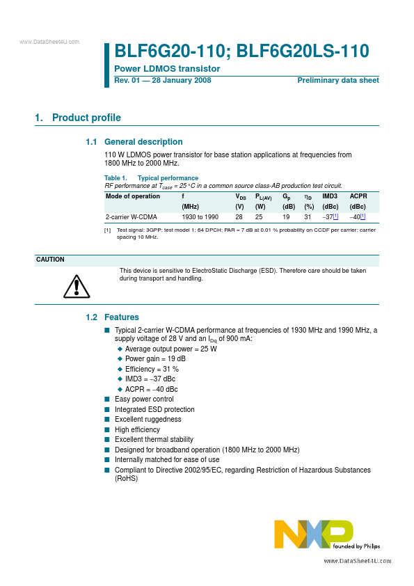
110 W LDMOS power transistor for base station applications at frequencies from 1800 MHz to 2000 MHz.
Table 1.
Typical performance RF performance at Tcase = 25 °C in a common source class-AB production test circuit.
| Part number | BLF6G20LS-110 |
|---|---|
| Manufacturer | NXP Semiconductors |
| File Size | 110.85 KB |
| Description | Power LDMOS transistor |
| Datasheet |
BLF6G20LS-110 Datasheet
|
|
|
|
| Part Number | Description | Manufacturer |
|---|---|---|
| BLF6G20LS-180RN | Power LDMOS Transistor | NXP |
| BLF6G20LS-180RN | Power LDMOS transistor | Ampleon |
| BLF6G20-180P | UHF power LDMOS transistor | NXP |
| BLF6G20-180RN | Power LDMOS Transistor | NXP |
| BLF6G20-180RN | Power LDMOS transistor | Ampleon |
| Part Number | Description |
|---|---|
| BLF6G20LS-140 | Power LDMOS transistor |
| BLF6G20-110 | Power LDMOS transistor |
| BLF6G20-180PN | Power LDMOS transistor |
| BLF6G20-230PRN | Power LDMOS transistor |
| BLF6G22-45 | Power LDMOS transistor |
The following content is an automatically extracted verbatim text from the original manufacturer datasheet and is provided for reference purposes only.