Datasheet Details
| Part number | UPA2750GR |
|---|---|
| Manufacturer | NEC |
| File Size | 67.76 KB |
| Description | SWITCHING N- AND P-CHANNEL POWER MOS FET |
| Datasheet |
 UPA2750GR Datasheet UPA2750GR Datasheet
|
|
|
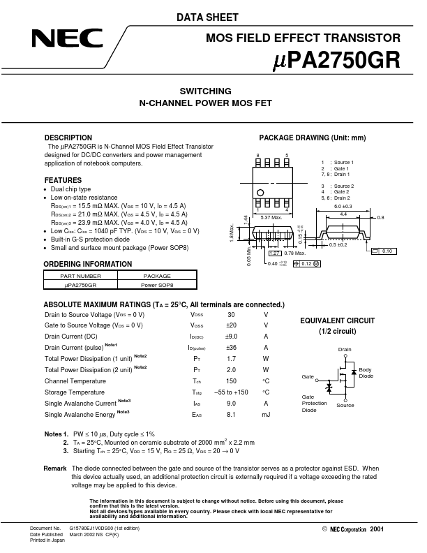
The µPA2750GR is N-Channel MOS Field Effect Transistor designed for DC/DC converters and power management application of notebook computers.
8 5 1 ; Source 1 2 ; Gate 1 7, 8 ; Drain 1 3 ; Source 2 4 ; Gate 2 5, 6 ; Drain 2 1 4 5.37 Max.
0.05| Part number | UPA2750GR |
|---|---|
| Manufacturer | NEC |
| File Size | 67.76 KB |
| Description | SWITCHING N- AND P-CHANNEL POWER MOS FET |
| Datasheet |
UPA2750GR Datasheet
|
|
|
|
| Part Number | Description | Manufacturer |
|---|---|---|
| uPA2755AGR | SWITCHING N-CHANNEL POWER MOS FET | Renesas |
| uPA2757GR | SWITCHING N-CHANNEL POWER MOS FET | Renesas |
| UPA2719AGR | P-CHANNEL POWER MOS FET | Renesas |
| UPA2731UT1A | P-CHANNEL POWER MOSFET | Renesas |
| UPA2735GR | P-channel MOSFET | Renesas |
| Part Number | Description |
|---|---|
| UPA2751GR | SWITCHING N- AND P-CHANNEL POWER MOS FET |
| UPA2752GR | SWITCHING N- AND P-CHANNEL POWER MOS FET |
| UPA2753GR | SWITCHING N- AND P-CHANNEL POWER MOS FET |
| UPA2754GR | SWITCHING N- AND P-CHANNEL POWER MOS FET |
| UPA2755GR | SWITCHING N- AND P-CHANNEL POWER MOS FET |
The following content is an automatically extracted verbatim text from the original manufacturer datasheet and is provided for reference purposes only.