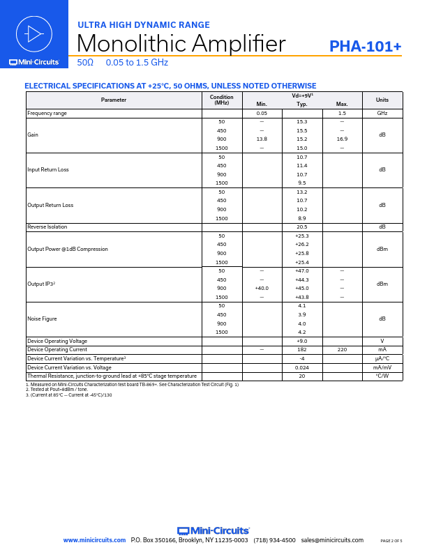
Description
RF-IN
RF-OUT
and DC-IN 4
3 RF-OUT & DC-IN 2 GROUND
GND
1 RF-IN
Function
Pin Number
Description
RF IN
1
RF input pin.This pin requires the use of an external DC blocking capacitor chosen for the frequency of operation.RF-OUT and DC-IN
3
RF output and bias pin.DC voltage is present on this pin; therefore a DC blocking capacitor is necessary for proper operation.An RF choke is needed to feed DC bias without loss of RF signal due to the bias connection, as shown in “Recommended App
Features
- Feature
Broad Band: 0.05 to 1.5 GHz
Advantages
Broadband covering primary wireless communications bands: Cellular, PCS, LTE
Extremely High IP3 Versus DC power Consumption +45 dBm typical at 0.9 GHz
The PHA-101+ matches industry leading IP3 performance relative to device size and power consumption. The combination of the design and E-PHEMT Structure provides enhanced linearity over a broad frequency range as evidence in the IP3 being typically 20 dB above the P 1dB point. This feature makes th.
 PHA-101+-Mini-Circuits.pdf