Description
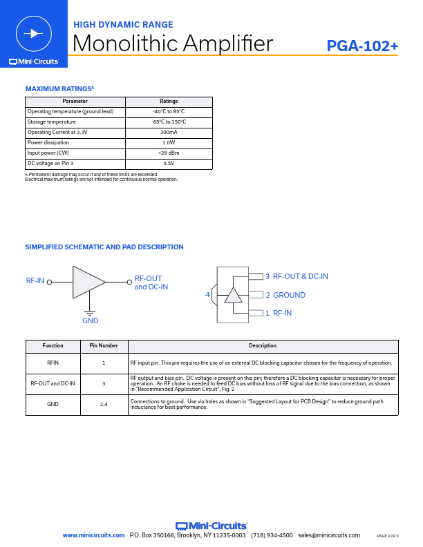
RF-IN
RF-OUT
and DC-IN 4
GND
3 RF-OUT & DC-IN 2 GROUND 1 RF-IN
Function RFIN
RF-OUT and DC-IN GND
Pin Number
Description
1
RF input pin.This pin requires the use of an external DC blocking capacitor chosen for the frequency of operation.RF output and bias pin.DC voltage is present on this pin; therefore a DC blocking capacitor is necessary for proper
3
operation.An RF choke is needed to feed DC bias without loss of RF signal due to the bias connection, as shown
in “Recommended A
Features
- Feature
Broad Band: 0.05 to 6.0 GHz
High IP3 Versus DC power Consumption: 33 dBm typical at 2 GHz at +3.3V Supply Voltage and only 83mA
No External Matching Components Required
Low Noise Figure: 2.3 dB up to 0.8 GHz
Advantages
Broadband covering primary wireless communications bands: Cellular, PCS, LTE, WiMAX
The PGA-102+ provides good IP3 performance relative to device size and power consumption. The combination of the design and E-PHEMT Structure provides enhanced linearity over a broad frequ.

 PGA-102+-Mini-Circuits.pdf