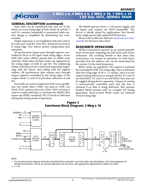
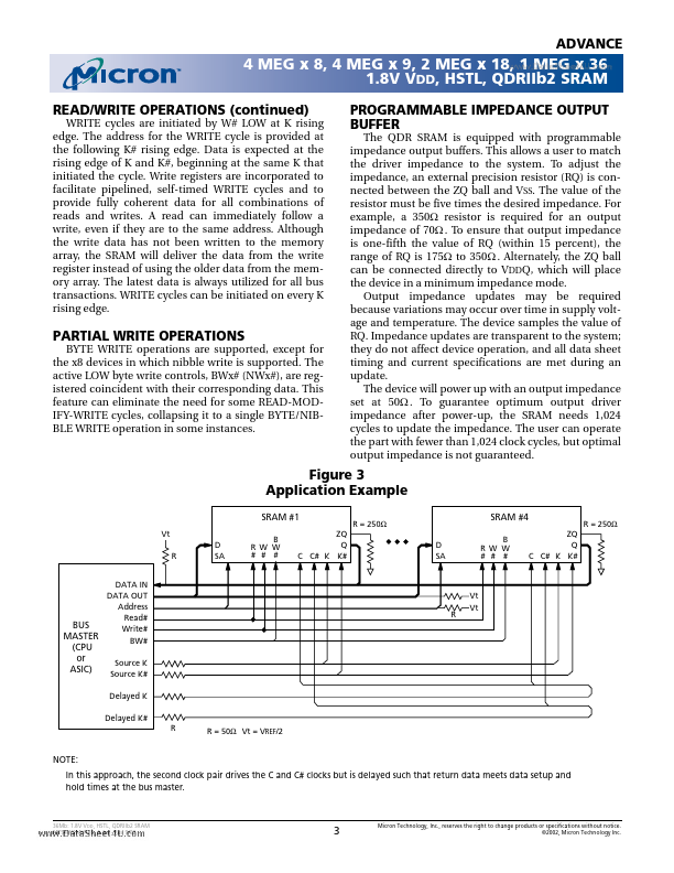
Description
4 Meg x 8, QDRIIb2 FBGA 4 Meg x 9, QDRIIb2 FBGA 2 Meg x 18, QDRIIb2 FBGA 1 Meg x 36, QDRIIb2 FBGA
OPTIONS
Clock Cycle Timing 4ns (250 MHz) 5ns (200 MHz) 6ns (167 MHz) 7.5ns (133 MHz)
Configurations 4 Meg x 8 4 Meg x 9 2 Meg x 18 1 Meg x 36
Package 165-ball, 15mm x 17mm FBGA
NOTE:
MARKING1
-4 -5 -6 -7.5
MT54W4MH8B MT54W4MH9B MT54W2MH18B MT54W1MH36B F
1. A Part Marking Guide for the FBGA devices can be found on Micron’s Web site
http://www.micron.com/numbe
Features
- DLL circuitry for accurate output data placement
MT54W4MH8B MT54W4MH9B MT54W2MH18B MT54W1MH36B
Figure 1 165-Ball FBGA.
- Separate independent read and write data ports with concurrent transactions.
- 100 percent bus utilization DDR READ and WRITE operation.
- Fast clock to valid data times.
- Full data coherency, providing most current data.
- Two-tick burst counter for low DDR transaction size.
- Double data rate operation on read and write.
 MT54W4MH8B_MicronTechnology.pdf