The following content is an automatically extracted verbatim text
from the original manufacturer datasheet and is provided for reference purposes only.
View original datasheet text
SMD Type
MOS Field Effect Transistor 2SK2111
MOSFICET
Features
Low on-resistance RDS(on)=0.6 MAX.@VGS=4.0V,ID=0.5A High switching speed
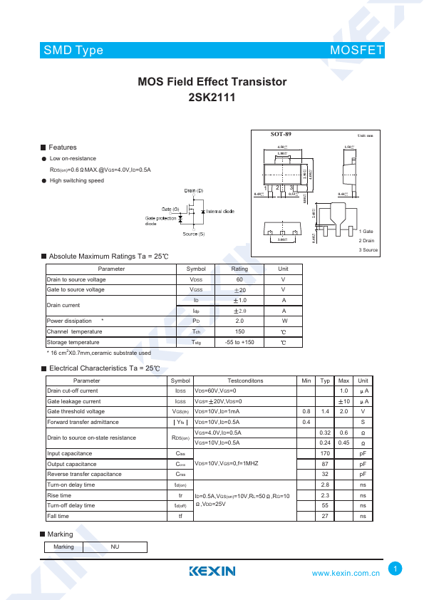
SOT-89
4.50+0.1 -0.1
1.80+0.1 -0.1
12 3
0.48+0.1 -0.1
0.53+0.1 -0.1
+0.12.50 -0.1
+0.14.00 -0.1
Unit: mm 1.50+0.1
-0.1
0.44+0.1 -0.1
+0.10.80 -0.1
+0.12.60 -0.1
3.00+0.1 -0.1
Absolute Maximum Ratings Ta = 25
Parameter Drain to source voltage Gate to source voltage
Drain current
Power dissipation * Channel temperature Storage temperature * 16 cm2X0.7mm,ceramic substrate used
Symbol VDSS VGSS ID Idp PD Tch Tstg
Rating 60 20 1.0 2.0 2.
 2SK2111 Datasheet